
Report:
Sophisticated CMP Technology with In-Line Optical-Thickness Verification for Shallow-Trench-Isolation Formation in GAAFETs with Multilayered Si/SiGe Superlattices
Yuji Kasashima†
 , Takashi Matsukawa
, Atsushi Yagishita, and Yoshihiro Hayashi
, Takashi Matsukawa
, Atsushi Yagishita, and Yoshihiro Hayashi
Semiconductor Frontier Research Center, National Institute of Advanced Industrial Science and Technology (AIST)
16-1 Onogawa, Tsukuba, Ibaraki 305-8569, Japan
†Corresponding author

A sophisticated chemical mechanical polishing (CMP) technology with in-line optical-thickness verification was developed for shallow-trench isolation formation in gate-all-around field-effect transistors with a multilayered Si/SiGe superlattice. The CMP tools were equipped with in-line optical critical dimension (OCD) measurement and a torque current monitor of the CMP turn-table motor for endpoint detection (EPD). In this study, model-based OCD fitting was applied to estimate the thicknesses of complex multilayered films: a SiN stopper on a thin SiO2 buffer layer over a Si/SiGe/Si/SiGe/Si/SiGe superlattice epitaxially grown on a Si substrate. Immediately after the CMP with the electrical EPD and the in-line OCD measurement, the over-polished thickness of the SiN stopper was within 3 nm on the fin-patterned Si/SiGe superlattice despite the change in the SiO2–CMP rate during continuous wafer processing. This nondestructive CMP control method improves the efficiency and quality of the CMP process in GAAFET fabrication.
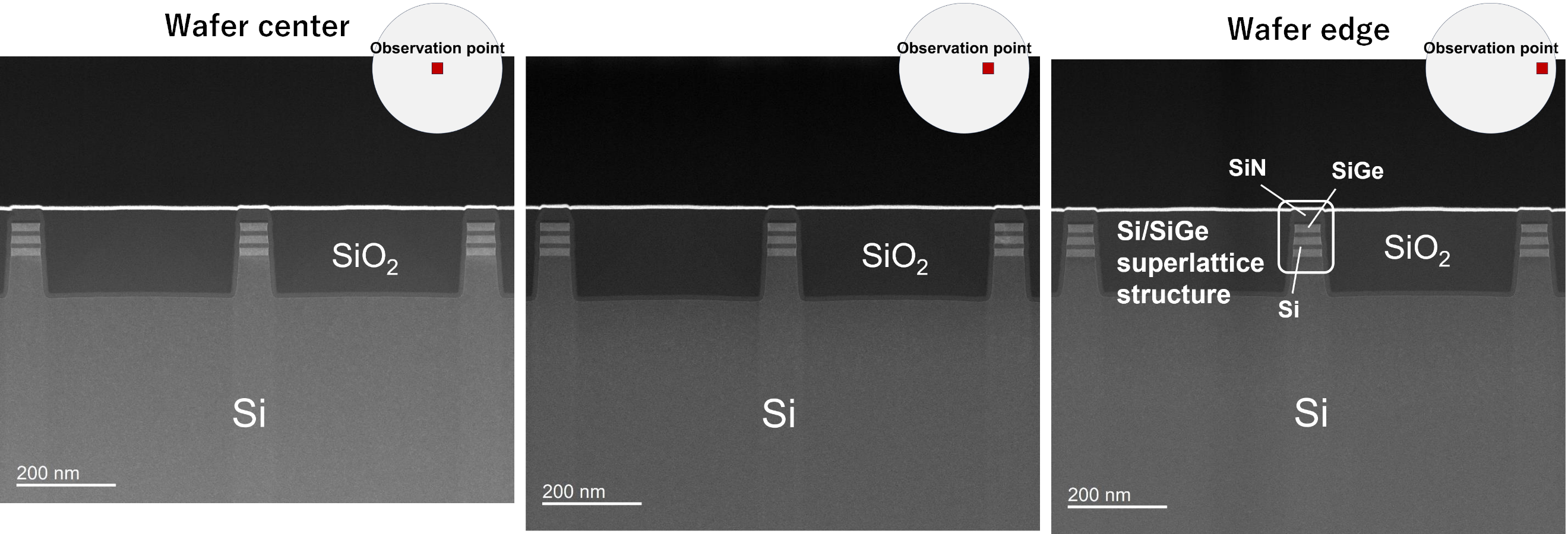
Cross-sectional TEM images after STI SiO2 CMP
1. Introduction
Fin field-effect transistors have been developed for 22 nm to 5 nm technology nodes, whereas gate-all-around field-effect transistors (GAAFETs) are employed at 3 nm and below. In GAAFET architectures, fin-patterned Si nanosheets are fully surrounded by high-\({k}\)/metal-gate stacks 1,2,3,4,5,6,7. Electrical isolation is achieved using shallow trench isolation (STI) in the Si substrate, formed via chemical mechanical polishing (CMP) of deposited SiO\(_2\).
CMP has been developed to flatten the surface of films deposited over a non-flattened underlayer, such as for STI, tungsten contact plugs, and copper or cobalt damascene interconnects 8,9,10,11,12,13,14,15,16,17,18,19. STI consists of trenches formed in the Si substrate around the active areas and filled with SiO\(_2\) for isolation. For fabrication of planar FETs, the STI CMP process has been developed 20. For STI formation in GAAFET fabrication, planarization is required for the SiO\(_2\) film that has been deposited on the fin-patterned Si/SiGe superlattices with a SiN CMP stopper film and the trenches in the Si substrate 21,22,23. Here, not only must the surface of the SiO\(_2\) film be flattened but also the thickness of the SiN stopper film on the superlattice must be precisely controlled after CMP. This is because, to construct the STI structure with the fin height built as designed, the amount of subsequent SiO\(_2\) recess etching is affected by the SiN film thickness.
The easiest method to evaluate the residual thicknesses of the SiO\(_2\) and SiN stopper layers after CMP is destructive cross-sectional observation using scanning electron microscopy (SEM) and/or transmission electron microscopy (TEM). This is valuable for optimizing the polishing conditions, such as the polishing speed and uniformity, but evaluating the uniformity at many locations across a 300 mm wafer is a time-consuming process and the wafer cannot be reused in the subsequent integration processes.
In this study, we developed a non-destructive process control method for the STI SiO\(_2\) CMP in GAAFET fabrication by combining in-situ monitoring of the motor torque current for the turntable in a polishing unit with in-line optical critical dimension (OCD) measurement on the fin-patterned Si/SiGe superlattice immediately after CMP. The main advantages of this method are as follows. (1) Rapid evaluation: the residual thickness of the SiN stopper layer and the dishing depth of SiO\(_2\) after the CMP process can be evaluated instantly, reducing the turnaround time. (2) High precision: the thickness of the SiN stopper layer can be accurately controlled within approximately 3 nm, ensuring process uniformity. (3) Non-destructive: measurements were performed without damaging the wafer, allowing it to be reused in subsequent processes. (4) Process stability: by combining motor-current endpoint detection (EPD) and OCD measurements, consistent results can be achieved even during consecutive wafer processing. Here, the dimension estimation process of the model-based OCD fitting is a key sequence for the complicated multilayer fin-shaped structure of the SiN/SiO\(_2\)/SiGe/Si/SiGe/Si/SiGe/Si substrate.
2. Experimental
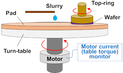
Fig. 1. Schematic of polishing process for STI SiO\(_2\) CMP.
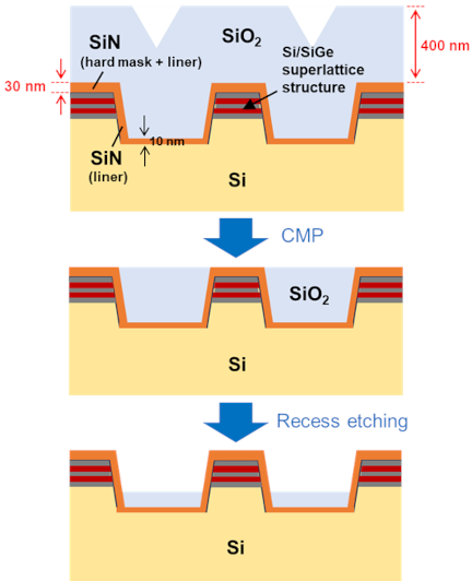
Fig. 2. Schematic of STI SiO\(_2\) CMP process and recess etching of SiO\(_2\).
As shown in Fig. 1, conventional CMP equipment (F-REX300X, EBARA) was used, in which the motor current of the turn-table in the polishing unit was monitored for in-situ EPD. The motor current reflected the friction condition between the polished surface and polishing pad on the turn-table and was changed by the surface roughness and/or appearance of a new material such as a SiN stopper film.
Figure 2 shows a schematic diagram of the STI CMP process on the fin-patterned substrate. The fin pattern was fabricated on 300 mm wafers with the Si/SiGe film, such as Si (2 nm)/SiGe (15 nm)/Si (10 nm)/SiGe (15 nm)/Si (10 nm)/SiGe (15 nm), epitaxially grown on a Si substrate. The Si/SiGe superlattice film and trenches in the Si substrate were patterned via reactive ion etching using a 20 nm-thick SiN film as a hard mask, and a 10 nm-thick SiN liner was deposited. Therefore, the initial SiN thickness on the Si/SiGe superlattice was 30 nm. The SiN film on the fin-patterned Si/SiGe superlattice acted as a SiO\(_2\) CMP stopping layer. Subsequently, a SiO\(_2\) film was deposited to a thickness of 400 nm to bury the trenches.
In the CMP process, a polyurethane polishing pad (IKONIC4131UH, NITTA DuPont) and a slurry of ceria particles (STI2305, Versum Materials) were used at a flow rate of 300 mL/min. The average polishing pressure was set at 243 hPa. The rotations of the polishing table and polishing head were set to 70 rpm and 71 rpm, respectively. The typical polishing rates of the blanket SiO\(_2\) film and SiN film were approximately 120 and 14 nm/min, respectively, preserving the CMP selectivity of SiO\(_2\) to SiN at 8.6. After the CMP of the SiO\(_2\) film, the SiO\(_2\) in the trenches was recess-etched, resulting in the fin of the Si/SiGe superlattice film with STI. The fin structure with the designed height was obtained after the STI SiO\(_2\) CMP was stopped on the SiN film without over-polishing.
The 3D structured test element group (TEG) patterns were created with a constant pitch to estimate 3D features such as the fin width, SiN film thickness on the top of the fin, and SiO\(_2\) film thickness buried between the fins. Using the TEG pattern, the SiN thickness and dishing depth immediately after CMP in the designated areas were evaluated instantly using an OCD measurement instrument (i550, NOVA). The OCD instrument was directly connected to the CMP equipment, and a wafer was placed across the wafer ports of the CMP equipment and OCD instrument.
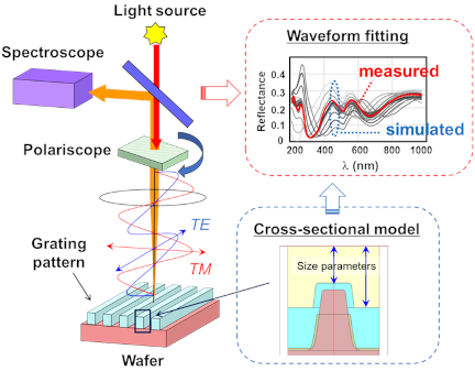
Fig. 3. Schematic of OCD measurement.
As shown in Fig. 3, the OCD measurement scheme was based on normal-incidence spectroscopic metrology using the patterns as a one-dimensional diffraction grating 24,25,26,27,28. By using a cross-sectional pattern model, the theoretical spectrum of the reflected wave from the incident light with two different polarization angles was simulated. The values of the parameters set in the model were gradually changed, and the theoretical spectrum was repeatedly simulated for each structure. The set of calculated results was then stored in a spectrum library. The dimensional values of the parameters were estimated by fitting the measured spectra to a library.
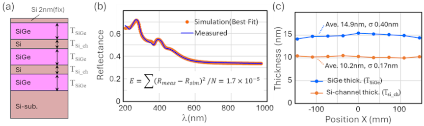
Fig. 4. Modelling Si/SiGe superlattice structure for constructing the OCD model of the STI structure: (a) Si/SiGe superlattice structure, (b) comparison between the measured spectrum for the superlattice structure and the simulated spectrum with best-fit thickness parameters, and (c) distribution of the SiGe and Si channel-thickness parameters across the wafer obtained via parameter fitting.
In a previous study of modelling STI structures for OCD, periodic Si pillars filled with SiO\(_2\) were investigated 28. For the purpose of expanding OCD measurement for the STI formation process in GAAFET fabrication, the Si/SiGe superlattice structure essential for the GAA structure definition and the SiN hardmask layer for protection of the superlattice from the CMP overpolish were newly added to the CMP model.
3. Results and Discussions
3.1. OCD Measurement for STI Formation in GAAFETs
First, the Si/SiGe superlattice structure for constructing the OCD model of the STI structure was modeled as shown in Fig. 4(a). The thickness parameters for the SiGe and Si channel layers (\(T_{\mathit{SiGe}}\) and \(T_{\mathit{Si\_ch}}\), respectively) were considered as the fitting parameters in the model. Note that the thicknesses of the three SiGe layers were assumed to be the same and expressed by the single variable \(T_\mathit{SiGe}\), and those for the two Si layers were assumed to be the same and expressed by the single variable \(T_\mathit{Si}\). The dielectric function of the SiGe films was estimated in advance using spectroscopic ellipsometry 29. Fig. 4(b) shows the results of the waveform comparison between the measured spectrum of the superlattice structure and the simulated spectrum with the best-fit thickness parameters. The sample number of wavelength \(N\) was set to 75 in the spectrum simulation. The fitting error, \(E\), estimated using the mean square of the difference between the measured reflectance, \(R_\mathit{meas}\), and the simulated reflectance, \(R_\mathit{sim}\), was set as low as \(1.7{\times}10^{-5}\). Fig. 4(c) shows the distribution of the SiGe and Si channel-thickness parameters, \(T_{\mathit{SiGe}}\) and \(T_{\mathit{Si\_ch}}\), across the 300 mm wafer obtained by parameter fitting. \(T_{\mathit{SiGe}}\) and \(T_{\mathit{Si\_ch}}\) were set to 15 nm and 10 nm, respectively, in the epitaxial growth process; hence, the results indicated that the Si/SiGe superlattice structure was successfully measured using OCD and that the thickness variation across the wafer was negligible. Thus, the thicknesses of the Si and SiGe layers were fixed in the model construction as follows.
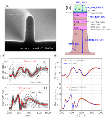
Fig. 5. OCD model construction of fin structure with Si/SiGe superlattice after Fin RIE process. (a) Cross-sectional SEM of the fin structure. (b) OCD model of the fin structure. (c) Simulated spectra with variation of all the dimensional parameters in Fig. 5(b). (d) Comparison between measured and simulated spectra with best-fit dimensional parameters.
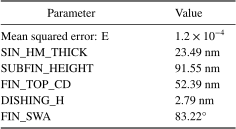
Before constructing the OCD model of the fin structure with the Si/SiGe superlattice after the STI CMP process, the model after the Fin RIE process was constructed. Figs. 5(a) and (b) show cross-sectional SEM images of the fin structure and OCD model, respectively. Based on the results shown in Fig. 4(c), the SiGe and Si channel thicknesses were fixed in the model. Fig. 5(c) shows the simulated spectra with variations in all the dimensional parameters shown in Fig. 5(b) and the measured spectrum. The spectra of both transverse electric (TE) and transverse magnetic (TM) polarizations were simulated. Fig. 5(d) shows a comparison of the measured and simulated spectra with the best-fit dimensional parameters. A summary of the fitting parameters shown in Fig. 5(d) is provided in Table 1. For the validation of the model and the fitting results, a comparison between the cross-sectional SEM image and the result of model fitting for the target structure is shown in Fig. 6. The model dimensions reproduce the actual structure well, although a slight difference is recognized because the position of the cross-sectional observation is not exactly the same as that of the OCD measurement.
Table 1. Summary of fitting parameters in Fig. 5(d).
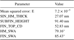
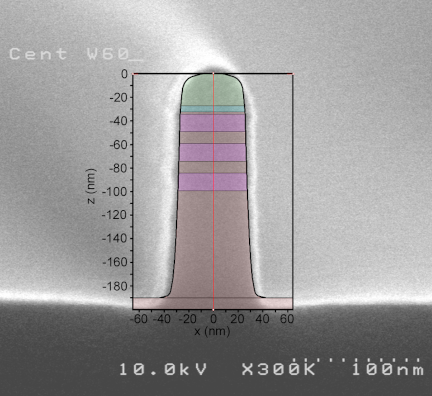
Fig. 6. Comparison between the OCD model fitted by the parameters in Table 1 and the cross-sectional SEM Fig. 5(a). The dimensions obtained from the fitted model reproduce the target structure well, although a slight difference is recognized because the position of the cross-sectional observation is not exactly the same as that of the OCD measurement.
Finally, an OCD model of the fin structure with a Si/SiGe superlattice after STI CMP was developed. In the STI CMP process, monitoring of the top SiN hard-mask thickness is quite important since the over-polish exceeding the SiN thickness would cause damage in the Si/SiGe superlattice structure essential for the GAA channel definition. Thus, an OCD model that provides the SiN hard-mask thickness together with the total fin height was developed. In the OCD model shown in Fig. 7(a), the thickness values of the superlattice were fixed. Fig. 7(b) shows the simulated spectra with variations in the SiN hard-mask thickness, i.e., SIN_HM_THICK. The SiN thickness variation from 10 nm to 40 nm is within the possible variation range due to the CMP over-polish. The simulated spectrum changes significantly with the change in SiN thickness. This result clarifies that the OCD measurement had high sensitivity to the SiN thickness, which is the most critical parameter of the STI CMP process. Fig. 7(c) shows the simulated spectra with variations in all the structural parameters in Fig. 7(b) and the measured spectrum. Fig. 7(d) compares the measured and simulated spectra with the best-fit dimensional parameters. A summary of the fitting parameters in Fig. 7(d) is provided in Table 2. The fitting error \(E\) was maintained below \(4{\times}10^{-4}\).
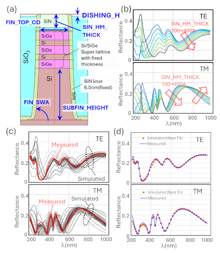
Fig. 7. OCD model of fin structure with Si/SiGe superlattice after the STI CMP process. (a) OCD model of the fin structure. (b) Simulated spectra with variation of SiN hard-mask thickness. (c) Simulated spectra with variations in all the structure parameters in Fig. 7(b). (d) Comparison between measured and simulated spectra with best-fit dimensional parameters.
Table 2. Summary of fitting parameters in Fig. 7(d).
3.2. STI Formation in GAAFETs
Figure 8 shows a typical waveform of the motor current of the turn-table in the polishing unit and its differential signal during the CMP process. Two signal increases were observed for the current waveform. The first increase in the signal observed at approximately 190–230 s reflected the gradual planarization of the initial non-flattened SiO\(_2\) film. After 230 s, the SiO\(_2\) film was fully planarized and the current signal became constant. The second increase at approximately 280–310 s reflected the gradual appearance of the SiN stopping layer. At approximately 310 s, the current signal became constant again, reflecting the condition that the SiN film appeared fully on the entire surface of the 300 mm wafer. In other words, this is EPD, which is detected at the zero-cross point of the differential signal.
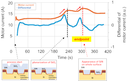
Fig. 8. Typical waveform of the motor current of the turn-table in the polishing unit and its differential signal.
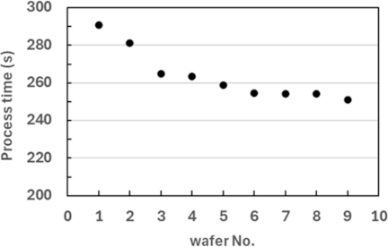
Fig. 9. Change in the process time when nine wafers were consecutively processed.
In this experiment, nine wafers were processed using EPD. Fig. 9 shows the change in the CMP process time using EPD. The process time decreased with an increase in the number of wafers processed, indicating that the CMP rate of SiO\(_2\) increased with the number of wafers processed. Therefore, EPD is mandatory to control over-polishing and to check the thickness using the in-line OCD immediately after CMP.
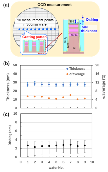
Fig. 10. (a) Schematic of OCD measurement, measurement result of (b) SiN thickness and its standard deviation over average, and (c) dishing after STI SiO\(_2\) CMP.
Figure 10(a) illustrates the positions of the OCD measurements used to check the residual thickness of the SiN film on the fin-patterned Si/SiGe superlattice film, as well as the dishing depth of SiO\(_2\) in the area between the fin patterns. The thickness and depth were observed at 10 points along the direction of the wafer diameter immediately after CMP. Fig. 10(b) shows the average SiN thicknesses with error bars as a function of the number of wafers processed. The error bars reflect the variation of the measured values at the 10 points. The SiN thickness was kept almost constant at approximately 27 nm through nine wafers that were continuously processed. Variations such as the ratio of the standard deviation to the average were within 6%. Because the initial SiN thickness was fixed at 30 nm, the over-polished thickness was suppressed to approximately 3 nm (\(=30\)–27 nm) after the CMP. Fig. 10(c) shows the dishing depth of the SiO\(_2\) film over the STI area without the fin-patterned Si/SiGe superlattices. The error bars reflect the variation of the measured values at the 10 points. The dishing depth was within approximately 3 nm at 10 points on each of the nine 300 mm wafers continuously processed.
Note that, as shown in Fig. 9, the SiO\(_2\) polishing rate was not constant, but increased with the number of wafers processed. Although the CMP rate changed during consecutive processing, the over-polishing thickness of the SiN film and the dishing depth of the SiO\(_2\) STI film were confirmed to be controlled within 3 nm by in-line OCD measurements immediately after CMP with the EPD system. Fig. 11 shows the cross-sectional TEM images obtained after STI CMP using the EPD system. It is clearly seen that the SiO\(_2\) thin film was fully planarized among the fin-patterned Si/SiGe superlattices in the whole wafer.
4. Summary
One of the challenges in GAAFET fabrication is STI formation by SiO\(_2\) CMP, which separates the complicated fin patterns of the multilayer Si/SiGe superlattice. This requires precise control of the SiN stopper thickness to ensure that the fin height is built as designed and uniform planarization of the SiO\(_2\) film in STI without dishing.
We developed a smart process control technology for STI SiO\(_2\) CMP with in-situ torque current monitoring EPD systems and in-line OCD measurements. The main advantages of the developed method are rapid evaluation, high precision, non-destructive measurement, and process stability. These advantages enhance the efficiency and quality of the CMP process in GAAFET fabrication.
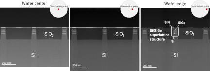
Fig. 11. Cross-sectional TEM images of the fin-patterned Si/SiGe superlattice buried in the STI SiO\(_2\) film planarized at the locations of the center, middle, and periphery of a 300 mm wafer.
Acknowledgments
This paper is based on results obtained from Research and Development Project of the Enhanced Infrastructures for Post 5G Information and Communication Systems subsidized by the New Energy and Industrial Technology Development Organization (NEDO), Project No.JPNP20017. We thank M. Yamagishi, M. Katou, and K. Ohta (AIST) for their helpful cooperation and discussions.
- [1] Q. Zhang et al., “New structure transistors for advanced technology node CMOS ICs,” Nat. Sci. Rev., Vol.11, No.3, Article No.nwae008, 2024. https://doi.org/10.1093/nsr/nwae008
- [2] C. Auth et al., “A 22nm high performance and low-power CMOS technology featuring fully-depleted tri-gate transistors, self-aligned contacts and high density MIM capacitors,” Proc. Symp. VLSI Technol., pp. 131-132, 2012. https://doi.org/10.1109/VLSIT.2012.6242496
- [3] S. Natarajan et al., “A 14nm logic technology featuring 2nd-generation FinFET, air-gapped interconnects, self-aligned double patterning and a 0.0588 µm ^2 2 SRAM cell size,” Proc. IEEE Int. Electron Devices Meet. (IEDM), pp. 3.7.1-3.7.3, 2014. https://doi.org/10.1109/IEDM.2014.7046976
- [4] S. Natarajan, M. Agostinelli, S. Akbar, M. Bost, A. Bowonder, V. Chikarmane et al., “A 10nm high performance and low-power CMOS technology featuring 3rd generation FinFET transistors, self-aligned quad patterning, contact over active gate and cobalt local interconnects,” Proc. IEEE Int. Electron Devices Meet. (IEDM), pp. 29.1.1-29.1.4, 2017.
- [5] C. Pan et al., “Technology/system codesign and benchmarking for lateral and vertical GAA nanowire FETs at 5-nm technology node,” IEEE Trans. Electron Devices, Vol.62, No.10, pp. 3125-3132, 2015. https://doi.org/10.1109/TED.2015.2461457
- [6] R. Stevenson, “Rise of the nanowire transistor,” IEEE Spectr., Vol.53, No.2, pp. 9-11, 2016. https://doi.org/10.1109/MSPEC.2016.7419783
- [7] Y.-C. Huang et al., “GAAFET versus pragmatic FinFET at the 5nm Si-based CMOS technology node,” IEEE J. Electron Devices Soc., Vol.5, No.3, pp. 164-169, 2017. https://doi.org/10.1109/JEDS.2017.2689738
- [8] F. B. Kaufman et al., “Chemical-mechanical polishing for fabricating patterned W metal features as chip interconnects,” J. Electrochem. Soc., Vol.138, No.11, pp. 3460-3464, 1991. https://doi.org/10.1149/1.2085434
- [9] M. A. Fury, “Milestones in a quarter century of CMP - plenary,” ECS Trans., Vol.19, No.7, pp. 3-11, 2009. https://doi.org/10.1149/1.3123769
- [10] Y. Hayashi and S. Takahashi, “Nitride-masked polishing (NMP) technique for surface planarization of interlayer-dielectric films,” Jpn. J. Appl. Phys., Vol.32, No.3R, pp. 1060-1063, 1993. https://doi.org/10.1143/JJAP.32.1060
- [11] Y. Hayashi et al., “Ammonium-salt-added silica slurry for the chemical mechanical polishing of the interlayer dielectric film planarization in ULSI’s,” Jpn. J. Appl. Phys., Vol.34, No.2S, pp. 1037-1042, 1995. https://doi.org/10.1143/JJAP.34.1037
- [12] R. Srinivasan, P. V. Dandu, and S. V. Babu, “Shallow trench isolation chemical mechanical planarization: A review,” ECS J. Solid State Sci. Technol., Vol.4, No.11, pp. P5029-P5039, 2015. https://doi.org/10.1149/2.0071511jss
- [13] G. Banerjee and R. L. Rhoades, “Chemical mechanical planarization historical review and future direction,” ECS Trans., Vol.13, No.4, pp. 1-19, 2008. https://doi.org/10.1149/1.2912973
- [14] T. Rothe et al., “Real-time interfacial pressure prediction in CMP using machine learning surrogates of finite element simulations,” Int. J. Autom. Technol., Vol.19, No.5, pp. 879-889, 2025. https://doi.org/10.20965/ijat.2025.p0879
- [15] Y. Watanabe et al., “Study on CMP of carbon films using zirconia particles,” Int. J. Autom. Technol., Vol.19, No.5, pp. 913-920, 2025. https://doi.org/10.20965/ijat.2025.p0913
- [16] M. Uneda et al., “Investigation into chemical mechanical polishing mechanism of hard-to-process materials using a commercially available single-sided polisher,” Int. J. Autom. Technol., Vol.9, No.5, pp. 573-579, 2015. https://doi.org/10.20965/ijat.2015.p0573
- [17] T. Hayashi, T. Seri, and S. Kurokawa, “A novel particle sizing method for nano abrasives in CMP slurry by using fluorescent nano probe,” Int. J. Autom. Technol., Vol.11, No.5, pp. 754-760, 2017. https://doi.org/10.20965/ijat.2017.p0754
- [18] P. Wrschka et al., “Chemical mechanical planarization of copper damascene structures,” J. Electrochem. Soc., Vol.147, No.2, pp. 706-712, 2000. https://doi.org/10.1149/1.1393256
- [19] M. Krishnan, J. W. Nalaskowski, and L. M. Cook, “Chemical mechanical planarization: Slurry chemistry, materials, and mechanisms,” Chem. Rev., Vol.110, No.1, pp. 178-204, 2009. https://doi.org/10.1021/cr900170z
- [20] R. Srinivasan, P. V. R. Dandu, and S. V. Babu, “Shallow trench isolation chemical mechanical planarization: A review,” ECS J. Solid State Sci. Technol., Vol.4, No.11, Article No.P5029, 2015. https://doi.org/10.1149/2.0071511jss
- [21] Q. Zhang et al., “New structure transistors for advanced technology node CMOS ICs,” Nat. Sci. Rev., Vol.11, No.3, Article No.nwae008, 2024. https://doi.org/10.1093/nsr/nwae008
- [22] M. Zhang et al., “Performance improvements in GAA NSFET devices and circuits using a hybrid dual- kappa κ spacer strategy at 3 nm node and beyond,” ECS J. Solid State Sci. Technol., Vol.14, No.3, Article No.035001, 2025. https://doi.org/10.1149/2162-8777/adbebc
- [23] S. Kim et al., “Investigation of device performance for fin angle optimization in FinFET and gate-all-around FETs for 3 nm-node and beyond,” IEEE Trans. Electron Devices, Vol.69, No.4, pp. 2088-2093, 2022. https://doi.org/10.1109/TED.2022.3154683
- [24] W. Yang et al., “Line-profile and critical-dimension monitoring using a normal incidence optical CD metrology,” IEEE Trans. Semicond. Manuf., Vol.17, No.4, pp. 564-572, 2004. https://doi.org/10.1109/TSM.2004.835728
- [25] N. G. Orji et al., “Metrology for the next generation of semiconductor devices,” Nat. Electron., Vol.1, No.4, pp. 532-547, 2018. https://doi.org/10.1038/s41928-018-0150-9
- [26] C. Guo et al., “Integrated optical critical dimension metrology with Mueller matrix ellipsometry,” Thin Solid Films, Vol.768, Article No.139695, 2023. https://doi.org/10.1016/j.tsf.2023.139695
- [27] C. J. Raymond et al., “Multiparameter grating metrology using optical scatterometry,” J. Vac. Sci. Technol. B, Vol.15, No.2, pp. 361-368, 1997. https://doi.org/10.1116/1.589320
- [28] J. Hu et al., “Measurement of shallow trench isolation by normal incidence optical critical dimension technique,” J. Vac. Sci. Technol. B, Vol.22, No.3, pp. 1000-1005. https://doi.org/10.1116/1.1722039
- [29] N. Kumagai, T. Irisawa, and Y. Hayashi, “Spectroscopic ellipsometry characterization of ultra-thin Si layer sandwiched between SiGe layers for nano-sheet FET fabrication,” Proc. ICSI/ISTDM, pp. 189-190, 2025.
This article is published under a Creative Commons Attribution-NoDerivatives 4.0 Internationa License.