Report:
Sophisticated CMP Technology with In-Line Optical-Thickness Verification for Shallow-Trench-Isolation Formation in GAAFETs with Multilayered Si/SiGe Superlattices
Yuji Kasashima†
 , Takashi Matsukawa
, Atsushi Yagishita, and Yoshihiro Hayashi
, Takashi Matsukawa
, Atsushi Yagishita, and Yoshihiro Hayashi
Semiconductor Frontier Research Center, National Institute of Advanced Industrial Science and Technology (AIST)
16-1 Onogawa, Tsukuba, Ibaraki 305-8569, Japan
†Corresponding author

A sophisticated chemical mechanical polishing (CMP) technology with in-line optical-thickness verification was developed for shallow-trench isolation formation in gate-all-around field-effect transistors with a multilayered Si/SiGe superlattice. The CMP tools were equipped with in-line optical critical dimension (OCD) measurement and a torque current monitor of the CMP turn-table motor for endpoint detection (EPD). In this study, model-based OCD fitting was applied to estimate the thicknesses of complex multilayered films: a SiN stopper on a thin SiO2 buffer layer over a Si/SiGe/Si/SiGe/Si/SiGe superlattice epitaxially grown on a Si substrate. Immediately after the CMP with the electrical EPD and the in-line OCD measurement, the over-polished thickness of the SiN stopper was within 3 nm on the fin-patterned Si/SiGe superlattice despite the change in the SiO2–CMP rate during continuous wafer processing. This nondestructive CMP control method improves the efficiency and quality of the CMP process in GAAFET fabrication.
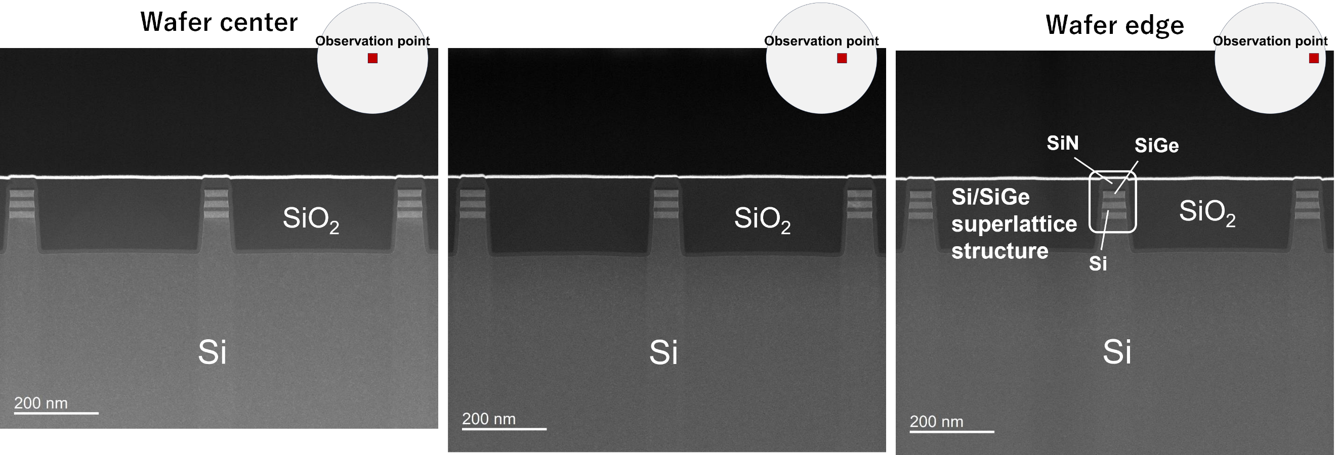
Cross-sectional TEM images after STI SiO2 CMP
- [1] Q. Zhang et al., “New structure transistors for advanced technology node CMOS ICs,” Nat. Sci. Rev., Vol.11, No.3, Article No.nwae008, 2024. https://doi.org/10.1093/nsr/nwae008
- [2] C. Auth et al., “A 22nm high performance and low-power CMOS technology featuring fully-depleted tri-gate transistors, self-aligned contacts and high density MIM capacitors,” Proc. Symp. VLSI Technol., pp. 131-132, 2012. https://doi.org/10.1109/VLSIT.2012.6242496
- [3] S. Natarajan et al., “A 14nm logic technology featuring 2nd-generation FinFET, air-gapped interconnects, self-aligned double patterning and a 0.0588 µm ^2 2 SRAM cell size,” Proc. IEEE Int. Electron Devices Meet. (IEDM), pp. 3.7.1-3.7.3, 2014. https://doi.org/10.1109/IEDM.2014.7046976
- [4] S. Natarajan, M. Agostinelli, S. Akbar, M. Bost, A. Bowonder, V. Chikarmane et al., “A 10nm high performance and low-power CMOS technology featuring 3rd generation FinFET transistors, self-aligned quad patterning, contact over active gate and cobalt local interconnects,” Proc. IEEE Int. Electron Devices Meet. (IEDM), pp. 29.1.1-29.1.4, 2017.
- [5] C. Pan et al., “Technology/system codesign and benchmarking for lateral and vertical GAA nanowire FETs at 5-nm technology node,” IEEE Trans. Electron Devices, Vol.62, No.10, pp. 3125-3132, 2015. https://doi.org/10.1109/TED.2015.2461457
- [6] R. Stevenson, “Rise of the nanowire transistor,” IEEE Spectr., Vol.53, No.2, pp. 9-11, 2016. https://doi.org/10.1109/MSPEC.2016.7419783
- [7] Y.-C. Huang et al., “GAAFET versus pragmatic FinFET at the 5nm Si-based CMOS technology node,” IEEE J. Electron Devices Soc., Vol.5, No.3, pp. 164-169, 2017. https://doi.org/10.1109/JEDS.2017.2689738
- [8] F. B. Kaufman et al., “Chemical-mechanical polishing for fabricating patterned W metal features as chip interconnects,” J. Electrochem. Soc., Vol.138, No.11, pp. 3460-3464, 1991. https://doi.org/10.1149/1.2085434
- [9] M. A. Fury, “Milestones in a quarter century of CMP - plenary,” ECS Trans., Vol.19, No.7, pp. 3-11, 2009. https://doi.org/10.1149/1.3123769
- [10] Y. Hayashi and S. Takahashi, “Nitride-masked polishing (NMP) technique for surface planarization of interlayer-dielectric films,” Jpn. J. Appl. Phys., Vol.32, No.3R, pp. 1060-1063, 1993. https://doi.org/10.1143/JJAP.32.1060
- [11] Y. Hayashi et al., “Ammonium-salt-added silica slurry for the chemical mechanical polishing of the interlayer dielectric film planarization in ULSI’s,” Jpn. J. Appl. Phys., Vol.34, No.2S, pp. 1037-1042, 1995. https://doi.org/10.1143/JJAP.34.1037
- [12] R. Srinivasan, P. V. Dandu, and S. V. Babu, “Shallow trench isolation chemical mechanical planarization: A review,” ECS J. Solid State Sci. Technol., Vol.4, No.11, pp. P5029-P5039, 2015. https://doi.org/10.1149/2.0071511jss
- [13] G. Banerjee and R. L. Rhoades, “Chemical mechanical planarization historical review and future direction,” ECS Trans., Vol.13, No.4, pp. 1-19, 2008. https://doi.org/10.1149/1.2912973
- [14] T. Rothe et al., “Real-time interfacial pressure prediction in CMP using machine learning surrogates of finite element simulations,” Int. J. Autom. Technol., Vol.19, No.5, pp. 879-889, 2025. https://doi.org/10.20965/ijat.2025.p0879
- [15] Y. Watanabe et al., “Study on CMP of carbon films using zirconia particles,” Int. J. Autom. Technol., Vol.19, No.5, pp. 913-920, 2025. https://doi.org/10.20965/ijat.2025.p0913
- [16] M. Uneda et al., “Investigation into chemical mechanical polishing mechanism of hard-to-process materials using a commercially available single-sided polisher,” Int. J. Autom. Technol., Vol.9, No.5, pp. 573-579, 2015. https://doi.org/10.20965/ijat.2015.p0573
- [17] T. Hayashi, T. Seri, and S. Kurokawa, “A novel particle sizing method for nano abrasives in CMP slurry by using fluorescent nano probe,” Int. J. Autom. Technol., Vol.11, No.5, pp. 754-760, 2017. https://doi.org/10.20965/ijat.2017.p0754
- [18] P. Wrschka et al., “Chemical mechanical planarization of copper damascene structures,” J. Electrochem. Soc., Vol.147, No.2, pp. 706-712, 2000. https://doi.org/10.1149/1.1393256
- [19] M. Krishnan, J. W. Nalaskowski, and L. M. Cook, “Chemical mechanical planarization: Slurry chemistry, materials, and mechanisms,” Chem. Rev., Vol.110, No.1, pp. 178-204, 2009. https://doi.org/10.1021/cr900170z
- [20] R. Srinivasan, P. V. R. Dandu, and S. V. Babu, “Shallow trench isolation chemical mechanical planarization: A review,” ECS J. Solid State Sci. Technol., Vol.4, No.11, Article No.P5029, 2015. https://doi.org/10.1149/2.0071511jss
- [21] Q. Zhang et al., “New structure transistors for advanced technology node CMOS ICs,” Nat. Sci. Rev., Vol.11, No.3, Article No.nwae008, 2024. https://doi.org/10.1093/nsr/nwae008
- [22] M. Zhang et al., “Performance improvements in GAA NSFET devices and circuits using a hybrid dual- kappa κ spacer strategy at 3 nm node and beyond,” ECS J. Solid State Sci. Technol., Vol.14, No.3, Article No.035001, 2025. https://doi.org/10.1149/2162-8777/adbebc
- [23] S. Kim et al., “Investigation of device performance for fin angle optimization in FinFET and gate-all-around FETs for 3 nm-node and beyond,” IEEE Trans. Electron Devices, Vol.69, No.4, pp. 2088-2093, 2022. https://doi.org/10.1109/TED.2022.3154683
- [24] W. Yang et al., “Line-profile and critical-dimension monitoring using a normal incidence optical CD metrology,” IEEE Trans. Semicond. Manuf., Vol.17, No.4, pp. 564-572, 2004. https://doi.org/10.1109/TSM.2004.835728
- [25] N. G. Orji et al., “Metrology for the next generation of semiconductor devices,” Nat. Electron., Vol.1, No.4, pp. 532-547, 2018. https://doi.org/10.1038/s41928-018-0150-9
- [26] C. Guo et al., “Integrated optical critical dimension metrology with Mueller matrix ellipsometry,” Thin Solid Films, Vol.768, Article No.139695, 2023. https://doi.org/10.1016/j.tsf.2023.139695
- [27] C. J. Raymond et al., “Multiparameter grating metrology using optical scatterometry,” J. Vac. Sci. Technol. B, Vol.15, No.2, pp. 361-368, 1997. https://doi.org/10.1116/1.589320
- [28] J. Hu et al., “Measurement of shallow trench isolation by normal incidence optical critical dimension technique,” J. Vac. Sci. Technol. B, Vol.22, No.3, pp. 1000-1005. https://doi.org/10.1116/1.1722039
- [29] N. Kumagai, T. Irisawa, and Y. Hayashi, “Spectroscopic ellipsometry characterization of ultra-thin Si layer sandwiched between SiGe layers for nano-sheet FET fabrication,” Proc. ICSI/ISTDM, pp. 189-190, 2025.
This article is published under a Creative Commons Attribution-NoDerivatives 4.0 Internationa License.