
Paper:
Finite Element Analysis and Structural Modification of Catheter-Type Tactile Sensor Based on Polyvinylidene Fluoride Film
Kazuto Takashima*
 , Siyan Zhang*, Souichiro Nagano*, Makoto Takenaka**, and Kenji Ishida***
*Graduate School of Life Science and Systems Engineering, Kyushu Institute of Technology
2-4 Hibikino, Wakamatsu-ku, Kitakyushu, Fukuoka 808-0196, Japan
**Kagawa Prefectural Industrial Technology Center
587-1 Goto-cho, Takamatsu, Kagawa 761-8031, Japan
***Department of Applied Quantum Physics and Nuclear Engineering, Faculty of Engineering, Kyushu University
744 Motooka, Nishi-ku, Fukuoka, Fukuoka 819-0395, Japan

To enable quantitative palpation in vivo, we previously developed a catheter-type tactile sensor that uses a polyvinylidene fluoride (PVDF) film for detecting lesions based on surface changes. This study investigates the effects of the structural parameters for the sensor on the piezoelectric output. A coupled electrical-structural finite element analysis (FEA) is used to simulate the displacement of a sensor tip composed of silicone rubber layers, a PVDF film, and a plastic substrate film. The FEA results indicated that encapsulating the plastic film in rubber increased the output charge by approximately 56.5%, primarily due to enhanced strain caused by lateral expansion of the silicone rubber. Increasing the plastic film thickness and the distance between the neutral plane and the PVDF film was also found to increase the output charge. In addition, the sensor output was larger when the lower rubber layer was made thicker than the upper rubber layer. However, the material used for the substrate film was predicted to have the dominant effect on the sensor output, with the largest output being achieved for a film with a large Young’s modulus. To confirm the FEA results, we fabricated prototype sensors that used plastic, steel, and titanium films, and experimentally evaluated their performance. The results indicated that an appropriate choice of film material could increase the sensor output by 18.9 fold.
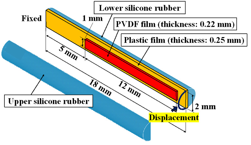
Schematic of simulation model for FEA
1. Introduction
Palpation 1 is used to detect changes in the shape and stiffness of tissues caused by disease by utilizing the excellent human sense of touch. It is applied to various parts of the body in clinical practice, but is limited to tissues accessible by the doctor’s hands. Furthermore, because manual palpation is subjective, its interpretation and diagnostic accuracy depend on the doctor’s experience. Consequently, a minimally invasive approach that allows the quantitative assessment of shape and stiffness is desirable. Thin flexible medical devices such as catheters are widely used in the treatment and diagnosis of diseases because they require only narrow incisions to approach a lesion. A miniaturized catheter-type tactile sensor that can quantitatively measure internal tissues would enable the development of more accurate and minimally invasive diagnosis and treatment methods for not only blood vessels but also organs such as the ureter, bronchus, and ventricles.
Existing catheter-type tactile sensors measure force based on piezoresistance 1,2,3,4, capacitance 1,2, optical measurement 1,3,5,6, or pressure (e.g., using pressure-sensitive rubber) 7. In our previous research, we fabricated a catheter-type tactile sensor that uses polyvinylidene fluoride (PVDF) 8,9,10. PVDF 1,8,9,10,11,12,13,14,15,16,17,18,19,20,21,22,23,24 is an organic ferroelectric that exhibits a piezoelectric response. It is a promising material for catheter-type tactile sensors because of its flexibility, thinness, easy handling, low weight, low cost, high piezoelectric voltage sensitivity, responsiveness over a wide frequency range, durability, lack of lead, inertness to chemical agents, and ability to measure the stress rate (not stress).
The previously fabricated sensor had an outer diameter of 2 mm and was produced by embedding a PVDF film in silicone rubber. The performance of the sensor was evaluated by inserting it into a blood vessel model with bumpy lesion-like protrusions 8. We showed that the sensor output reflected the shape of the inner wall of the model, allowing the position of protrusions and the convexity interval for a rough surface to be determined (Fig. 1). The sensor output waveform exhibited transverse variations, indicating transverse vibrations of the sensor tip, which produced a distinctive output when the tip passed over a rough surface area. Such thin flexible tactile sensors can be applied not only for quantitative measurement of tissue palpation but also for industrial applications, such as in-pipe inspection using industrial endoscopes, earthworm-like robots 25,26, and snake-like robots 27 to prevent accidents related to aging and corroded pipes.
Moreover, we previously examined the frequency response of the sensor 9,10, which depends on the convexity interval of the surface in contact with the sensor. In these previous studies, we also proposed theoretical models for the sensor output (see Section 2.1 for details) to allow estimation of the sensor output before the fabrication of prototypes.
However, in our previous experiments 9,10, the output values measured using the prototype sensor were smaller than the theoretical values. Therefore, in the present study, we performed a finite element analysis (FEA) in order to optimize the sensor structure to maximize its output. First, we evaluated the effects on the sensor output of the silicone rubber layer, the thickness of the plastic substrate film and the rubber layer, and the film material. Based on the FEA results, we fabricated prototype sensors and evaluated their performance experimentally.
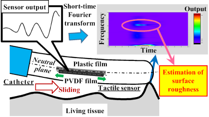
Fig. 1. Quantitative and minimally invasive palpation in vivo using catheter-type tactile sensor (e.g., convexity interval of rough surface). The root of the sensor is fixed inside a catheter.
2. Numerical Simulation
2.1. Theoretical Equations
Using the piezoelectric coefficients (\(d_{31}\), \(d_{32}\), and \(d_{33}\)), the output current (\(I\)) for the PVDF film in the sensor can be expressed as follows:
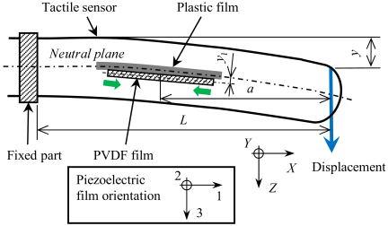
Fig. 2. Schematic representation of catheter-type tactile sensor whose root is fixed and whose tip is moved.
In clinical use, similar to other endovascular treatment devices such as guidewires, stents, and balloons, the sensor would be inserted into a catheter, and the root of the sensor would be fixed (Fig. 1). Assuming this situation, as illustrated in Fig. 2, the sensor is bent by a tip displacement \(y\), which is applied by the shaker at a frequency \(f\). Using a constant \(y_{0}\), \(y\) can be expressed as follows:
We ignore the resistance of the PVDF film to deformation and assume that the neutral plane is located at the center of the plastic film. Therefore, when the sensor is bent, the PVDF film away from the neutral plane becomes extended or compressed (Fig. 2). The insertion of a plastic substrate film increases the distance between the neutral plane of the sensor and the PVDF film (\(y_{1}\)). The orientation of the PVDF film embedded in the proposed sensor is illustrated in the inset in Fig. 2. The PVDF film is embedded to apply tensile stress (\(\sigma_{1}\) in Eq. \(\eqref{eq:eq1}\)) when the sensor is axially extended. Similar to our previous studies 9,10, the ratio between the amplitude of the output current (\(I_{0}\)) and \(y_{0}\) can be expressed as
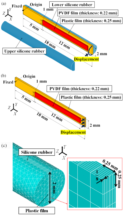
Fig. 3. Schematic diagram of simulation model for FEA. (a) With silicone rubber. (b) Without silicone rubber. (c) Final mesh size used in this study.
2.2. FEA Method
2.2.1. Simulation Model
In our previous papers 9,10, the measured sensor output was smaller than that obtained using Eq. \(\eqref{eq:eq3}\). We investigated the cause of this discrepancy using the FEA model shown in Fig. 3. In the model, the origin is located at the center and the root of the plastic film. FEA was performed using the software ANSYS Mechanical APDL 2023 R2 (ANSYS Inc.). The FEA model consists of PVDF and plastic films sandwiched between two silicone rubber layers. The PVDF and plastic films and the silicone rubber are assumed to be isotropic elastic materials. We neglect the thin electrodes and wires connected to the PVDF film in the actual prototype sensors. The cross sections of the upper and lower rubber layers are semi-cylindrical with a radius of 1 mm. These components are joined using Boolean operations to form a single sensor structure.
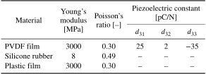
The PVDF film is modeled using SOLID226 a, which supports an electrostatic-structural combination. SOLID226 is a three-dimensional, 20-node coupled-field finite element available in ANSYS. It is used for multiphysics analysis. The element is applicable to piezoelectric analysis, enabling the coupled formulation of mechanical displacement and electric potential fields. It captures both direct and converse piezoelectric effects. The plastic film and the rubber layers are modeled using homogeneous structural solid elements (SOLID186 b). The parameters for each material are shown in Table 1. The \(+Z\)- and \(-Z\)-directions refer to the up and down directions, respectively.
Table 1. Characteristics of materials used in sensor [12, 28, c, d].
2.2.2. Simulation Conditions
Similar to the case shown in Fig. 2, the root of the sensor was constrained in all directions, and the tip of the sensor was displaced by \(-1\) mm along the \(Z\)-direction (Fig. 3). In the model with a rubber layer, the displacement was applied to the curved edge on the top surface of the upper rubber layer. In the model without a rubber layer, the displacement was applied to the line of the tip on the top surface of the plastic film. The electric potential at all nodes of the upper and lower electrodes on the PVDF film was assumed to be 0 V. Similar to our previous research 11, the output charge was obtained by calculating the electric force on the electrodes under this assumption.
First, we changed the element number (sum of the element numbers for the plastic and PVDF films) from 768 to 49,152. The output charge gradually decreased as the number of elements increased; it became almost constant at around 6,000 elements. Therefore, we fixed the element number at 6,144 and evaluated the effects of various parameters on the output charge. Based on this mesh size, we automatically fixed the element number for the silicone rubber at 26,848 using the SMRTSIZE command. The final mesh size used in this study is shown in Fig. 3(c).
Using this simulation model, we evaluated the effects of the rubber layer, the plastic substrate film thickness, the rubber thickness, and the substrate film material on the sensor output charge. The details are given in the following sections.
2.2.3. Effect of Rubber Layer
We evaluated the effect of the rubber layer using the sensor model with and without silicone rubber. The cross sections of the upper and lower rubber layers were semi-cylindrical with a radius of 1 mm.
2.2.4. Effect of Plastic Film Thickness
We changed the plastic film thickness (along the \(Z\)-axis) from 0.125 mm to 0.5 mm in steps of 0.125 mm and examined the effect on the sensor output. We used the sensor with and without silicone rubber. The cross sections of the upper and lower rubber layers were semi-cylindrical with a radius of 1 mm.
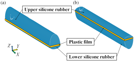
Fig. 4. Schematic diagrams of rubber layer with unequal thicknesses. (a) Upper/lower layer thicknesses: 2.0 mm / 0.5 mm. (b) Upper/lower layer thicknesses: 0.5 mm / 2.0 mm.
2.2.5. Effect of Rubber Thickness
We changed the maximum thickness of the upper and lower silicone rubber layers along the \(Z\)-direction individually from 0.5 mm to 2.0 mm in steps of 0.25 mm (Fig. 4) and evaluated the effect on the sensor output. The maximum thickness of the silicone rubber layers along the \(Y\)-direction was fixed at 2 mm. The cross section of each rubber layer was elliptical. The thickness of the plastic film was 0.25 mm.
2.2.6. Effect of Substrate Film Material
For Eq. \(\eqref{eq:eq3}\), we assumed that the neutral plane is located at the center of the plastic film. Consequently, Eq. \(\eqref{eq:eq3}\) does not depend on the type of film material or properties such as its elastic modulus. We replaced the plastic film with materials that had a larger Young’s modulus (3–534.4 GPa) 29 and examined the effect on the sensor output. We used the sensor with and without silicone rubber. The tested materials were titanium and steel. For the FEA model, we also considered lead, bismuth tin, aluminum, duralumin, gold, glass (flint), silver, brass, palladium, manganin, copper, invar, constantan, platinum, nickel, tungsten, and tungsten carbide in order to evaluate the effects of the Young’s modulus. Note that the Poisson’s ratio for these materials was different from that for the plastic film.
2.3. Results and Discussion
2.3.1. Effect of Rubber Layer
The sensor output with and without silicone rubber was 0.238 nC and 0.152 nC, respectively. Encapsulating the plastic film in the rubber increased the output charge by approximately 56.5%.
The normal strain for the PVDF and plastic films along the \(X\)-direction with and without silicone rubber is shown in Fig. 5. In Fig. 5(a), the silicone rubber is not shown to better illustrate the strain distribution. As illustrated in Fig. 5, the normal strain for the PVDF film along the \(X\)-direction with silicone rubber was larger than that without silicone rubber. Therefore, because \(\sigma_{1}\) also became large, the first term in Eq. \(\eqref{eq:eq1}\) increased.
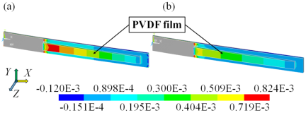
Fig. 5. Normal strain in \(X\)-direction. (a) With silicone rubber. (b) Without silicone rubber.
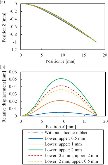
Fig. 6. (a) Deflection distribution for plastic film. (b) Relative displacement along \(Z\)-axis with respect to case without rubber.
The deflection distribution at the upper plane of the plastic film (\(Y=0\) mm) is shown in Fig. 6. As shown in Fig. 6, the central deflection of the sensor with silicone rubber along the \(+Z\)-direction was larger than that without rubber. Because the Poisson’s ratio for the rubber was 0.49, the volume change was small when the sensor was bent. Therefore, when the lower rubber layer was compressed along the \(X\)-direction, it extended along the \(Z\)-direction. As a result, the PVDF film extended along the \(X\)-axis, as shown in Fig. 5(a).
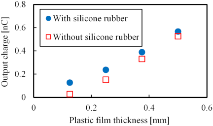
Fig. 7. Relationship between output charge and plastic film thickness.
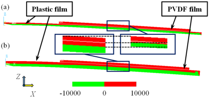
Fig. 8. Normal strain in \(X\)-direction (with silicone rubber). Plastic film thickness of (a) 0.25 mm and (b) 0.5 mm. Insets show magnified views.
2.3.2. Effect of Plastic Film Thickness
As shown in Fig. 7, as the thickness of the plastic film increased from 0.125 mm to 0.5 mm, the output charge of the sensor both with and without silicone rubber increased. The normal strain along the \(X\)-axis at \(Y=0\) mm is shown in Fig. 8. The silicone rubber is not shown to better illustrate the strain distribution. When the thickness of the plastic film increased, the distance between the neutral plane (the boundary between the red and green regions in Fig. 8) and the PVDF film increased. Therefore, because the normal strain for the PVDF film along the \(X\)-axis increased, the output charge also increased. On the other hand, as the thickness of the plastic film increased, the effect of the rubber layer became smaller.
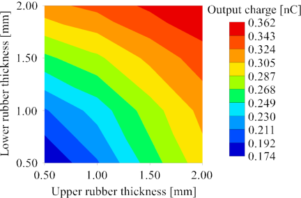
Fig. 9. Effect of upper and lower rubber layer thicknesses on output charge.
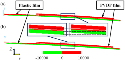
Fig. 10. Normal strain in \(X\)-direction. (a) Upper/lower layer thicknesses: 0.5 mm / 2 mm. (b) Upper/lower layer thicknesses: 2 mm / 0.5 mm. Insets show magnified views.
2.3.3. Effect of Rubber Thickness
The relationship between the rubber thickness and the output charge is shown in Fig. 9. When the thicknesses of the upper and lower rubber layers were the same and the total thickness increased, the output charge gradually increased (Fig. 9). However, note that the sensor diameter should be as small as possible to facilitate the application of the sensor in the human body. The output charge increase could be due to the increase in the central deflection of the plastic film along the \(+Z\)-direction (green line in Fig. 6) and the increase in the strain along the \(X\)-direction. On the other hand, when the thicknesses of the upper and lower rubber layers were unequal, a thicker lower rubber layer increased the sensor output. For example, when the thicknesses of the upper and lower silicone rubber layers were 0.5 mm and 2.0 mm, respectively, the sensor output was 0.318 nC. When the thicknesses of the upper and lower silicone rubber layers were 2.0 mm and 0.5 mm, respectively, the sensor output was 0.298 nC (6.39% smaller). The normal strain along the \(X\)-axis at \(Y=0\) mm is shown in Fig. 10. The silicone rubber is not shown to better illustrate the strain distribution. One reason for the difference could be similar to that described in Section 2.3.2, namely the increase in the strain for the PVDF film along the \(X\)-direction caused by the increase in the distance between the neutral plane (the boundary between the red and green regions in Fig. 10) and the PVDF film.
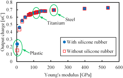
Fig. 11. Relationship between Young’s modulus and output charge.
2.3.4. Effect of Substrate Film Material
The effect of the substrate film material is shown in Fig. 11. As can be seen, the output charge for sensors both with and without silicone rubber increased when a material with a higher elastic modulus than that for plastic was used. When the elastic modulus was large, the output charge was larger than those presented in Sections 2.3.1, 2.3.2, and 2.3.3. This indicates that the effect of the substrate film material is larger than those of the other parameters. The strain distributions along the \(X\)-direction for plastic, titanium (Young’s modulus: 115.7 GPa, Poisson’s ratio: 0.321), and steel (Young’s modulus: 216 GPa, Poisson’s ratio: 0.3) films are shown in Fig. 12. The silicone rubber is not shown to better illustrate the strain distribution. The tensile strain on the surface increased with increasing elastic modulus. As a result, the tensile strain in the PVDF film also became large. For Eq. \(\eqref{eq:eq3}\), we assumed that the neutral plane is located at the center of the plastic film. However, when the elasticity of the film was small, the neutral plane shifted and the output charge decreased. Furthermore, in the range of 3 GPa to 100 GPa, the change in charge was large, whereas in the range of 100 GPa to 534.4 GPa, it was small. On the other hand, as the Young’s modulus increased, the effect of the rubber layer became smaller.
As described above, the sensor output can be increased by attaching silicone rubber and changing the film material. To confirm these FEA results, we fabricated prototype sensors that used plastic, steel, and titanium films, respectively.
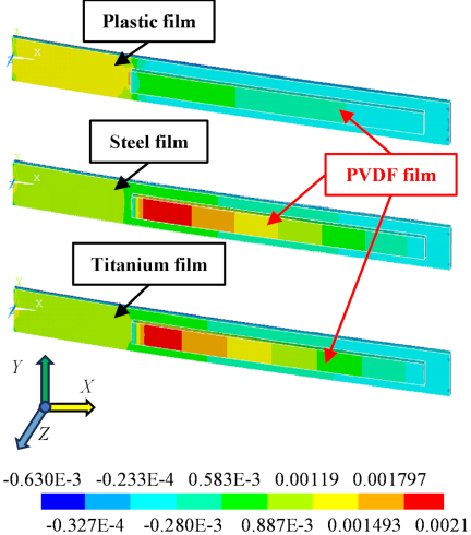
Fig. 12. Distribution of strain along \(X\)-axis (with silicone rubber).
3. Experiment
3.1. Prototype Tactile Sensor
A schematic representation and a photograph of the prototype sensors used in this study are shown in Fig. 13. We fabricated three types of samples, denoted as samples A and \(\mathrm{A'}\) (plastic), B and \(\mathrm{B'}\) (steel), and C and \(\mathrm{C'}\) (titanium). We fabricated two samples for each material to examine the effects of sensor manufacturing errors. Figs. 13(b), (c), and (d) show the average and standard deviation of the outer diameter from ten measurements obtained using a micrometer for the three types of sample, respectively. The outer diameters of samples \(\mathrm{A'}\), \(\mathrm{B'}\), and \(\mathrm{C'}\) were \(2.4\pm0.0\) mm, \(2.6\pm0.0\) mm, and \(2.4\pm0.0\) mm, respectively. There were manufacturing errors because the sensors were manufactured manually.
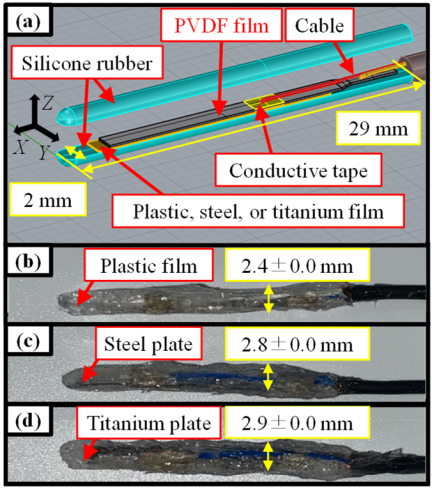
Fig. 13. Prototype tactile sensor based on PVDF film. (a) Schematic diagram. Photographs of samples (b) A, (c) B, and (d) C.
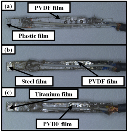
Fig. 14. Prototype tactile sensor based on PVDF film without silicone rubber. Photographs of samples (a) A, (b) B, and (c) C without silicone rubber.
Similar to our previous studies 9,10, for sample A, a piezoelectric film (Kureha Corporation, K0711-40AS-L20; total thickness: 0.22 mm, width: 5 mm, length: 20 mm, electrode surface area: 48 mm\(^{2})\) and two plastic films (KOKUGO Co., Ltd., 107-12306, total thickness: 0.25 mm) cut into 2 mm \(\times\) 27 mm pieces were glued together with elastic binder and attached to the lower silicone rubber layer (Shin-Etsu Chemical Co., Ltd., KE-106), as shown in Fig. 13(a). The piezoelectric film (hereafter simply referred to as the PVDF film) consisted of two overlaid PVDF sheets (individual thickness: 40 μm). We connected the film electrode to a shielded flexible signal cable using a conductive adhesive. Finally, we attached the upper silicone rubber layer using an adhesive for silicone rubber (MISUMI Corporation, BONDS). For samples B and C, we replaced the plastic film with steel (MISUMI Corporation, SFGSMW0.25, thickness: 0.25 mm) and titanium (Nilaco Corp., TI-453401, thickness: 0.25 mm), respectively. The steel and titanium films were cut into 2 mm \(\times\) 27 mm pieces. We also evaluated samples A, B, and C without silicone rubber (Fig. 14) to examine the effect of the rubber layer, which is ignored in Eq. \(\eqref{eq:eq3}\).
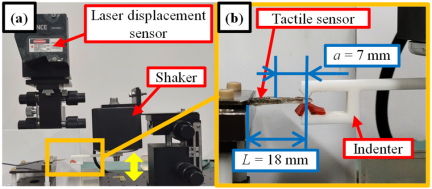
Fig. 15. (a) Photograph of experimental equipment. (b) Close-up view.
3.2. Experimental Method
Similar to our previous studies 9,10, we examined the sensor frequency response using the experimental apparatus shown in Fig. 15. The tip of the sensor, whose base was fixed in a jig, was vibrated by an indenter attached to a shaker and the output from the sensor was measured. The distance from the indenter contact position to the fixed part of the sensor and the center of the PVDF film was set to \(L=18\) mm and \(a=7\) mm, respectively (Fig. 15(b)). An oscilloscope in conjunction with a charge amplifier (NF Corporation, LI-76 e; gain: \(10^{6}\) V/A (DC to 20 kHz)) was used to determine the sensor output voltage. In our previous study 10, we showed that the input impedance of our sensors was considerably larger (\(>2\) M\(\Omega\)) than that of the amplifier (about 1 k\(\Omega\) at 400 Hz, gain: \(10^{6}\) V/A). Therefore, the effect of the input impedance of the amplifier on the measurements of the sensor output would be small. The movement of the indenter measured by a laser displacement sensor (Keyence Corporation, LK-G5000V, LK-H150) was also acquired by the oscilloscope.
Experiments were performed three times at each frequency. The measurement frequency was in the range of 10 Hz to 1,000 Hz, which is similar to that (20 Hz to 200 Hz) used in our previously reported sensor insertion tests using a blood vessel model with an uneven surface 8. To eliminate the impact of electrical noise, the acquired sensor output and displacement were subjected to a fast Fourier transform. At the applied frequency, the sensor output and tip displacement amplitudes (\(I_{0}\) and \(y_{0}\), respectively) were determined, and the average and standard deviation from three measurements were calculated.
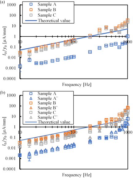
Fig. 16. Comparison of \(I_{0}/y_{0}\) for various sensors. (a) Without silicone rubber. (b) With silicone rubber.
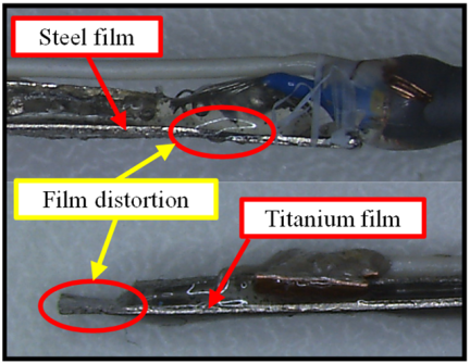
Fig. 17. Film distortion due to cutting.
3.3. Results and Discussion
The average and standard deviation of \(I_{0}/y_{0}\) for sensors without and with silicone rubber are depicted in Figs. 16(a) and (b), respectively. The theoretical values calculated from Eq. \(\eqref{eq:eq3}\) are also shown. Note that the theoretical values for all samples are the same because Eq. \(\eqref{eq:eq3}\) does not include the film material properties (e.g., elastic modulus) and does not consider the silicone rubber. Similar to the theoretical values, the measured value of \(I_{0}/y_{0}\) increases gradually with increasing frequency. As shown in Fig. 16, the outputs for samples B (\(\mathrm{B'}\)) and C (\(\mathrm{C'}\)) were the largest and the second largest, respectively, both with and without the silicone rubber. Consistent with the FEA results (Fig. 11), a substrate film with a large elastic modulus led to a large sensor output, similar to the theoretical values, and sensors with titanium and steel films had the largest outputs (increases of 9.0 and 18.9 fold, respectively, compared to plastic film). The sensor output was similar to the theoretical values only for a substrate film with a large elastic modulus because the above assumption regarding the neutral plane position for Eq. \(\eqref{eq:eq3}\) does not hold when the elastic modulus of the film is small.
As described above, although the trend of the sensor output could be easily estimated using Eq. \(\eqref{eq:eq3}\), more accurate output values, considering the film material, could be estimated using FEA. Therefore, the FEA proposed in this study can be used to assess the sensor output during design and before the fabrication of new catheter-type sensors with novel materials and shapes. Furthermore, similar FEA can be applied to other types of piezoelectric soft tactile sensors.
Similar to the FEA results presented in Sections 2.3.1, 2.3.2, and 2.3.4, attaching silicone rubber changed the sensor output. However, in contrast to the results in Sections 2.3.1, 2.3.2, and 2.3.4, the outputs from the sensors with silicone rubber were sometimes smaller than those without silicone rubber. One possible reason for this may be that the thicknesses of the upper and lower rubber layers were different due to manufacturing errors. Such thickness differences may have affected the neutral plane and thus the sensor output, as shown in Figs. 9 and 10.
As shown in Fig. 16(b), due to manufacturing errors (see Section 3.1 for details), the outputs were different between samples A and \(\mathrm{A'}\), B and \(\mathrm{B'}\), and C and \(\mathrm{C'}\), respectively. Moreover, as shown by the red oval in Fig. 17, the steel and titanium films had some distortion due to cutting. Future studies will investigate the most suitable cutting method for these films.
3.4. Future Challenges
The simulation model used in this study has several limitations that should be addressed in the future. First, because we ignored the nonlinearity, viscoelasticity, and inertia of the material used, large-deformation and high-frequency simulations could not be performed accurately. Second, because we applied a static displacement to the sensor tip along the \(Z\)-direction, twisting and dynamic deformation were not considered.
Moreover, there are several discrepancies between our evaluation conditions and real-world usage. For example, the verification method applied a forced displacement to the sensor, whereas in actual use, an increase in the stiffness of the sensor itself would likely result in less deflection under a given load. However, for practical applications of the sensor, we assume that the variation in its output frequency can be utilized to measure the surface roughness of a lesion (Fig. 1). Even if the displacement decreased, the output frequency would not change. Therefore, the effect of the displacement on the output frequency would be small even though the decrease in the sensor output could reduce the signal-to-noise ratio.
In the theoretical equations and FEA, based on the assumption that the sensor was inserted into a rigid catheter, the sensor root was fixed. However, this does not accurately reflect the actual conditions during clinical use because the catheter would also bend and the part constrained by the catheter would change. Therefore, to more accurately model clinical use, the theoretical equations and FEA model should be improved in the future. Narrowing (stepped or tapered) and softening (material change) of only the sensor tip 30 would better approximate the fixed-root situation and efficiently concentrate the vibration on the sensor tip to increase the signal-to-noise ratio.
4. Conclusion
In this research, we analyzed the structure of a catheter-type tactile sensor using FEA and experiments on prototype sensors to increase the sensor output. First, we evaluated the effects on the sensor output of the silicone rubber layer, the thickness of the plastic substrate film and the rubber layer, and the film material. The simulation results indicated that encapsulating the plastic film in the rubber increased the output charge by approximately 56.5%, which is primarily attributed to enhanced strain due to lateral expansion of the silicone rubber. Furthermore, increasing the plastic film thickness and the distance between the neutral plane and the PVDF film increased the sensor output. When the thicknesses of the upper and lower rubber layers were the same and the total thickness increased, the output charge gradually increased. In addition, when the upper and lower rubber layer thicknesses were unequal, a thicker lower rubber layer increased the sensor output. A substrate film with a large Young’s modulus led to a large sensor output. To confirm these FEA results, we fabricated prototype sensors that used plastic, steel, and titanium films, respectively, and evaluated them in experiments. The experiments confirmed that changing the film material could increase the sensor output by 18.9 fold.
Acknowledgments
This research was supported by JSPS KAKENHI Grant Number JP24H00422. The authors thank FORTE Science Communications (https://www.forte-science.co.jp/) for English language editing.
- [1] W. Othman et al., “Tactile sensing for minimally invasive surgery: Conventional methods and potential emerging tactile technologies,” Front. Robot. AI, Vol.8, Article No.705662, 2022. https://doi.org/10.3389/frobt.2021.705662
- [2] M. E. H. Eltaib and J. R. Hewit, “Tactile sensing technology for minimal access surgery–A review,” Mechatronics, Vol.13, No.10, pp. 1163-1177, 2003. https://doi.org/10.1016/S0957-4158(03)00048-5
- [3] B. Ren et al., “The critical technologies of vascular interventional robotic catheterization: A review,” IEEE Sens. J., Vol.23, No.24, pp. 30051-30069, 2023. https://doi.org/10.1109/JSEN.2023.3320356
- [4] M. Tanimoto et al., “Micro force sensor for intravascular neurosurgery and in vivo experiment,” Proc. IEEE 11th Annu. Int. Workshop Micro Electro Mech. Syst. (MEMS), pp. 504-509, 1998. https://doi.org/10.1109/MEMSYS.1998.659809
- [5] Y. Haga, T. Mineta, and M. Esashi, “Active catheter, active guide wire and related sensor systems,” Proc. 5th Biannu. World Autom. Congr., pp. 291-296, 2002. https://doi.org/10.1109/WAC.2002.1049455
- [6] P. Polygerinos et al., “Novel miniature MRI-compatible fiber-optic force sensor for cardiac catheterization procedures,” Proc. 2010 IEEE Int. Conf. Robot. Autom. (ICRA), pp. 2598-2603, 2010. https://doi.org/10.1109/ROBOT.2010.5509416
- [7] T. Sekitani, U. Zschieschang, H. Klauk, and T. Someya, “Flexible organic transistors and circuits with extreme bending stability,” Nat. Mater., Vol.9, No.12, pp. 1015-1022, 2010. https://doi.org/10.1038/nmat2896
- [8] K. Takashima et al., “Development of catheter-type tactile sensor composed of polyvinylidene fluoride (PVDF) film,” ROBOMECH J., Vol.6, Article No.19, 2019. https://doi.org/10.1186/s40648-019-0147-9
- [9] K. Takashima, M. Watanabe, K. Inoue, S. Horie, and K. Ishida, “Fabrication and evaluation of catheter-type tactile sensor composed of two polyvinylidene fluoride films,” 61st Annu. Conf. Soc. Instrum. Control Eng. (SICE), pp. 1165-1170, 2022. https://doi.org/10.23919/SICE56594.2022.9905774
- [10] K. Takashima, S. Nagano, M. Watanabe, and K. Ishida, “Characterization of catheter-type tactile sensor using polyvinylidene fluoride (PVDF) film,” J. Robot. Mechatron., Vol.36, No.4, pp. 899-908, 2024. https://doi.org/10.20965/jrm.2024.p0899
- [11] K. Takashima et al., “Measurement of the piezoelectric properties of vinylidene fluoride oligomer using pneumatic pressure for tactile sensors,” J. Solid Mech. Mater. Eng., Vol.6, No.10, pp. 975-988, 2012. https://doi.org/10.1299/jmmp.6.975
- [12] T. Okuyama, M. Sone, Y. Tanahashi, and M. Tanaka, “Palpation sensor using two PVDF films,” ICMIT 2009: Mechatron. Inf. Technol. (Proc. SPIE, Vol.7500), Article No.75000J, 2010. https://doi.org/10.1117/12.858316
- [13] I. Fujimoto, Y. Yamada, T. Maeno, T. Morizono, and Y. Umetani, “Identification of incipient slip phenomena based on the circuit output signals of PVDF film strips embedded in artificial finger ridges,” Trans. Soc. Instrum. Control Eng., Vol.40, No.6, pp. 648-655, 2004. https://doi.org/10.9746/sicetr1965.40.648
- [14] W. Feng, H. Wang, S. Guo, K. Wang, and X. Ye, “Design and experiments of a catheter side wall tactile sensor for minimum invasive surgery,” 2007 Int. Conf. Mechatron. Autom., pp. 1073-1078, 2007. https://doi.org/10.1109/ICMA.2007.4303697
- [15] Z. Chen, K.-Y. Kwon, and X. Tan, “Integrated IPMC/PVDF sensory actuator and its validation in feedback control,” Sens. Actuators A: Phys., Vol.144, No.2, pp. 231-241, 2008. https://doi.org/10.1016/j.sna.2008.01.023
- [16] M. Tanaka, “Sensor system for measuring human touch sensation,” J. Robot. Soc. Jpn., Vol.26, No.3, pp. 230-233, 2008 (in Japanese). https://doi.org/10.7210/jrsj.26.230
- [17] R. Kikuuwe, K. Nakamura, and M. Yamamoto, “Finger-mounted tactile sensor for evaluating surfaces,” J. Robot. Mechatron., Vol.24, No.3, pp. 430-440, 2012. https://doi.org/10.20965/jrm.2012.p0430
- [18] Z. Yi, Y. Zhang, and J. Peters, “Bioinspired tactile sensor for surface roughness discrimination,” Sens. Actuators A: Phys., Vol.255, pp. 46-53, 2017. https://doi.org/10.1016/j.sna.2016.12.021
- [19] X. L. Sun, J. P. Yan, Y. F. Li, and H. Liu, “Multi-frequency ultrasound transducers for medical applications: A survey,” Int. J. Intell. Robot. Appl., Vol.2, No.3, pp. 296-312, 2018. https://doi.org/10.1007/s41315-018-0057-7
- [20] K. Tsukagoshi, T. Hashimoto, and T. Koike, “Simultaneous measurement of swallowing sound and mechanomyogram of submental muscle with PVDF film,” 40th Annu. Int. Conf. IEEE Eng. Med. Biol. Soc. (EMBC), pp. 3310-3313, 2018. https://doi.org/10.1109/EMBC.2018.8512959
- [21] R. Lin et al., “Applications of flexible electronics related to cardiocerebral vascular system,” Mater. Today Bio, Vol.23, Article No.100787, 2023. https://doi.org/10.1016/j.mtbio.2023.100787
- [22] Q. Zhang et al., “Hierarchically structured hollow PVDF nanofibers for flexible piezoelectric sensor,” Chem. Eng. J., Vol.498, Article No.155661, 2024. https://doi.org/10.1016/j.cej.2024.155661
- [23] A. Kanwal et al., “A comprehensive review of piezoelectric BaTiO_{3}-based polymer composites for smart tactile sensing,” Emergent Mater., Vol.8, No.8, pp. 6137-6176, 2025. https://doi.org/10.1007/s42247-025-01208-3
- [24] R. Ybarra et al., “Advanced microstructured BaTiO_{3}-embedded PVDF-HFP/PEO film for enhanced triboelectric interface in self-sufficient energy generation and sensing,” ACS Omega, Vol.10, No.38, pp. 43450-43461, 2025. https://doi.org/10.1021/acsomega.5c01183
- [25] S. Horii and T. Nakamura, “An in-pipe mobile robot for use as an industrial endoscope based on an earthworm’s peristaltic crawling,” J. Robot. Mechatron., Vol.24, No.6, pp. 1054-1062, 2012. https://doi.org/10.20965/jrm.2012.p1054
- [26] R. Okuma, S. Matsuo, F. Ito, and T. Nakamura, “Development of a robot combining a hyper-extension unit and an earthworm-type robot enhancing propulsion and traction,” J. Robot. Mechatron., Vol.37, No.1, pp. 86-98, 2025. https://doi.org/10.20965/jrm.2025.p0086
- [27] Y. Suzuki, “Development of a tactile sensor for a snake robot,” J. Robot. Soc. Jpn., Vol.37, No.5, pp. 414-417, 2019 (in Japanese). https://doi.org/10.7210/jrsj.37.414
- [28] The Japan Society of Mechanical Engineers (Ed.), “JSME Mechanical Engineers’ Handbook DVD-ROM,” Maruzen Publishing, Co., Ltd., 2014 (in Japanese).
- [29] National Astronomical Observatory of Japan (Ed.), “Chronological Scientific Tables,” Vol.77, Maruzen Co. Ltd., 2003 (in Japanese).
- [30] J. Deng, O. Guasch, L. Zheng, T. Song, and Y. Cao, “Semi-analytical model of an acoustic black hole piezoelectric bimorph cantilever for energy harvesting,” J. Sound Vib., Vol.494, Article No.115790, 2021. https://doi.org/10.1016/j.jsv.2020.115790
- [a] ANSYS Website. https://ansyshelp.ansys.com/public/account/secured?returnurl=/////////Views/Secured/corp/v242/en/ans_elem/Hlp_E_SOLID226.html [Accessed February 13, 2026]
- [b] ANSYS Website. https://ansyshelp.ansys.com/public/account/secured?returnurl=/////////Views/Secured/corp/v242/en/ans_elem/Hlp_E_SOLID186.html [Accessed February 13, 2026]
- [c] Kureha Trading Website (in Japanese). https://www.kureha-trading.co.jp/catalog/ [Accessed February 13, 2026]
- [d] Shin-Etsu Chemical Website (in Japanese). https://www.silicone.jp/catalog/pdf/LiquidSiliconeRubbers-ind_J.pdf [Accessed February 13, 2026]
- [e] NF Website. https://www.nfcorp.co.jp/english/pro/mi/loc/pre/li_76/specifications.html [Accessed February 13, 2026]
This article is published under a Creative Commons Attribution-NoDerivatives 4.0 Internationa License.