
Research Paper:
Frequency Characteristics of High-Voltage Power Semiconductor Gate Drive Circuit Using Resonant Inductive Wireless Power Transfer
Ning Li*,†
 , Takeshi Shinkai*
, and Dong Yue**
*Tokyo University of Technology
1404-1 Katakuramachi, Hachioji, Tokyo 192-0982, Japan
†Corresponding author
**Institute of Advanced Technology for Carbon Neutrality, Nanjing University of Posts and Telecommunications
No.9 Wenyuan Road, Yadong New District, Nanjing 210023, China

This paper investigates the frequency characteristics of a high-voltage gate-drive circuit using resonant inductive wireless power transfer (RIWPT). In the proposed RIWPT system, both the control and carrier signals are transmitted simultaneously through magnetically coupled coils, then rectified and applied to the gate of a SiC MOSFET to ensure reliable switching operation. For given amplitudes of the control and carrier signals, the achievable transfer distance is analyzed at different carrier frequencies. For the 44-turn α-wound coil, with a 15-V control signal and a 30-V carrier signal, a maximum power transfer distance of 151 mm is obtained at a carrier frequency of approximately 260 kHz. For the 44-turn spiral coil, with the same control signal and a 10-V carrier signal, a maximum transfer distance of 200 mm is achieved at a carrier frequency of approximately 193 kHz. Both maximum transfer distances satisfy the required coil separation distance to ensure adequate insulation for a system operating at a high voltage of 28.3 kV. Furthermore, the frequency-dependent variation in the turn-on and turn-off times with respect to the carrier frequency and gate–source drive voltage is also investigated. Based on the analysis, an optimization is implemented through simulation. The optimized turn-on and turn-off time are significantly reduced to 14 µs and 7 µs, respectively. In this paper, the presented results are all based on electromagnetic simulations using Ansys Maxwell and circuit simulations using Keysight ADS. In our future work, experimental validation of the proposed RIWPT gate-drive system will be conducted to verify the simulation results and further evaluate its practical feasibility under high-voltage operating conditions.
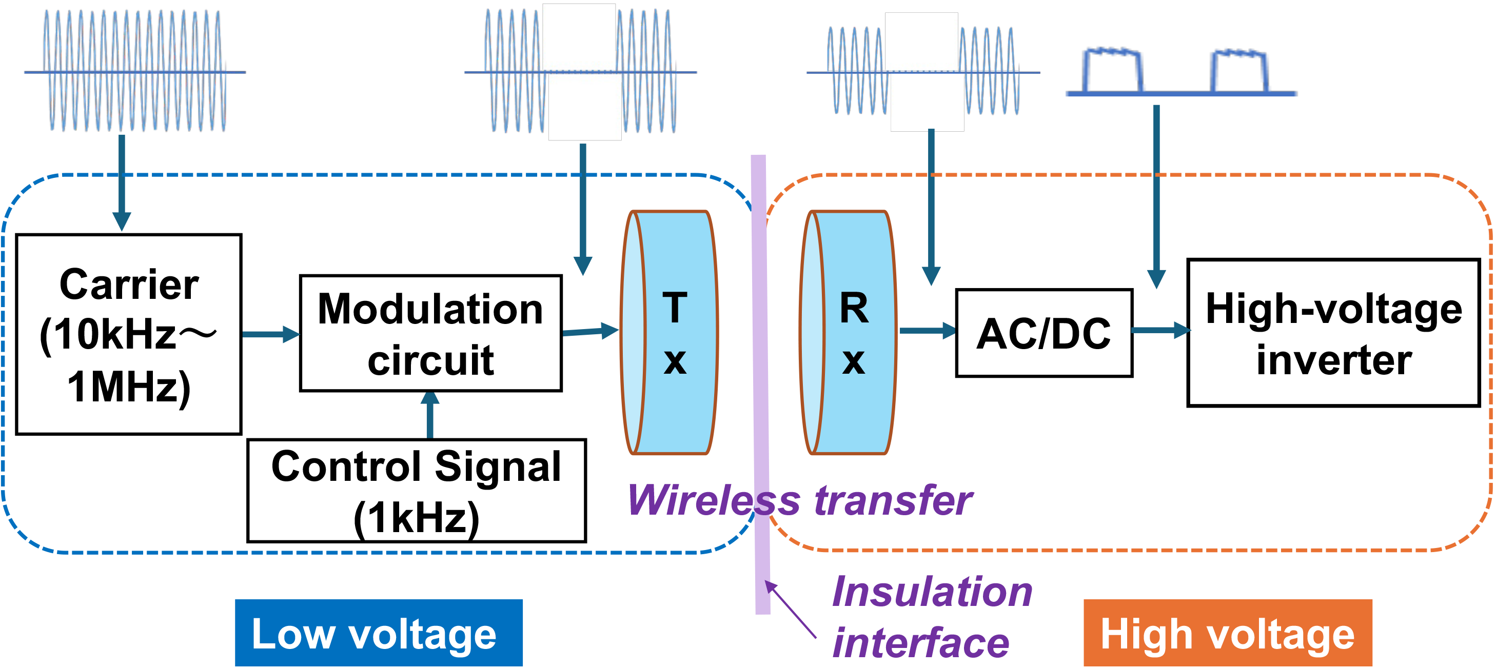
High-voltage wireless gate drivecircuit
1. Introduction
High-voltage power electronic systems require reliable galvanic isolation for gate-drive circuits to ensure safe and stable operation 1,2,3,4,5. Conventional isolation techniques, such as pulse transformers and optocouplers, face significant challenges in high-voltage environments, including limited insulation capability, increased parasitic effects, and reduced reliability under fast switching conditions 6,7. These limitations become more critical in emerging applications involving kilovolt-level operation, where both insulation distance and switching performance must be carefully balanced.
Wireless power transfer (WPT), particularly resonant inductive wireless power transfer (RIWPT), has recently emerged as a promising alternative for contactless gate driving due to its inherent galvanic isolation and structural flexibility 8. By utilizing magnetically coupled coils, RIWPT systems can simultaneously transfer energy and control signals without direct electrical connections. However, most existing studies primarily focus on power transfer efficiency or low-voltage applications, while limited attention has been given to high-voltage gate-drive systems and their associated frequency-dependent switching behavior.
In addition, prior work typically assumes fixed operating conditions, without systematically investigating the interdependence between carrier frequency, transfer distance, and switching dynamics 8. In practical high-voltage systems, these factors are strongly coupled: increasing carrier frequency can improve dynamic response but may degrade transfer distance, while gate-drive voltage levels directly influence switching speed through nonlinear gate-charge characteristics. This multidimensional trade-off has not been thoroughly analyzed or quantified in existing RIWPT-based gate-drive designs.
To address these challenges, this paper presents a high-voltage gate-drive circuit based on RIWPT, capable of simultaneously transmitting control and carrier signals through magnetically coupled coils. The main contributions of this work are summarized as follows:
-
・
Frequency-dependent transfer-distance characterization is systematically analyzed for high-voltage insulation requirements, revealing the existence of an optimal carrier frequency that maximizes transfer distance under fixed gate-drive conditions.
-
・
The coupled relationship between carrier frequency and switching performance is investigated, demonstrating that turn-on and turn-off times exhibit distinct and nontrivial dependencies on the gate–source voltage and operating frequency.
-
・
A comparative study of two widely used coil structures, namely the \(\alpha\)-wound coil and spiral coil, is conducted using electromagnetic simulation, highlighting their impact on coupling coefficient, parasitic parameters, and overall system performance.
-
・
Based on the above analysis, a design-oriented optimization strategy is proposed to balance transfer distance, switching speed, and gate-drive constraints, achieving improved switching performance while maintaining sufficient insulation for a 28.3-kV system.
The results show that, although an optimal carrier frequency exists for maximizing transfer distance, higher operating frequencies are required to reduce switching time, leading to an inherent trade-off between insulation capability and dynamic performance. These findings provide important design insights for high-voltage isolated gate-drive systems based on WPT.
The remainder of this paper is organized as follows. Section 2 presents the electromagnetic simulation and characterization of the 44-turn \(\alpha\)-wound and spiral coils. Section 3 describes the gate-drive circuit configuration and simulation setup. Section 4 investigates the frequency-dependent transfer characteristics and their impact on switching performance in the proposed high-voltage RIWPT system. Finally, Section 5 concludes the paper.
2. System Block Diagram and Coil Design
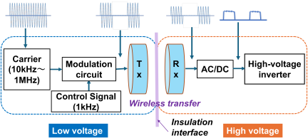
Fig. 1. Block diagram of gate drive circuit for high-voltage inverter adapting simultaneously wireless transfer both for control signal and power 8.
The block diagram of the simultaneous inductive WPT system both for the control and carrier signals is shown in Fig. 1. In this system, the carrier signal is modulated by the control signal, transmitted and received by the coupling coils, then rectified by the full-wave rectifier circuit, and finally applied to the gate of the SiC MOSFET, ensuring proper operation of the high-voltage gate drive circuit. The previous work in 8 primarily demonstrated a prototype of the concept, while in 9, a comprehensive electromagnetic design and performance evaluation of coils targeted at high-voltage gate drive applications has been studied. The key factors including coil geometry and coil shape have been investigated. However, the discussions are all at a fixed carrier frequency. Since the resonant frequency is also a key factor for the WPT system, it is necessary to investigate the frequency characteristics of the proposed prototype in 8.
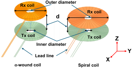
Fig. 2. Structure of \(\alpha\)-wound and spiral coils used in EM simulation. The \(\alpha\)-wound coil uses a two-layer structure, while spiral coil has a single-layer layout 9.
| Coil type | \(\alpha\)-wound | Spiral |
| Turns | 44 | 44 |
| Wind gap [mm] | 1 | 1 |
| Wind diameter [mm] | 1 | 1 |
| \(D_{\mathrm{in}}\) [mm] | 9.50 | 9.50 |
| \(D_{\mathrm{outer}}\) [mm] | 97.6 | 184 |
| Layer | 2 | 1 |
In this study, two widely used coil types, namely the \(\alpha\)-wound coil and spiral coil shown in Fig. 2, are investigated using Ansys Maxwell 10. The Tx and Rx coils used in the simulation are identical, each with an inner diameter of 9.5 mm. The wire diameter is 1 mm and the inter-turn gap is set to 1 mm. The simulation frequency range is set from 1 Hz to 1 MHz, with the skin effect taken into account. The physical geometry of the coils, including conductor diameter, number of turns, and inter-turn gap, is specified and summarized in Table 1. Copper is used as the conductor material, with a conductivity \(\sigma\) of \(5.8\times10^7\) S/m. Although no insulation layer was explicitly modeled, this omission does not directly affect conductor loss. The surrounding air domain and boundary conditions are configured to prevent truncation of the magnetic field.
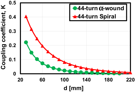
Fig. 3. Simulated coupling coefficient, \(k\), between Tx and Rx coils with separation distance for both 44-turn \(\alpha\)-wound and spiral coils.
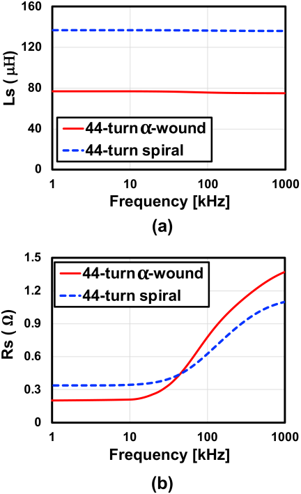
Fig. 4. Simulated self-inductance and parasitic resistance of the coils with respect to frequency. (a) Tx and Rx coils’ self-inductance, (b) Parasitic resistance 9.
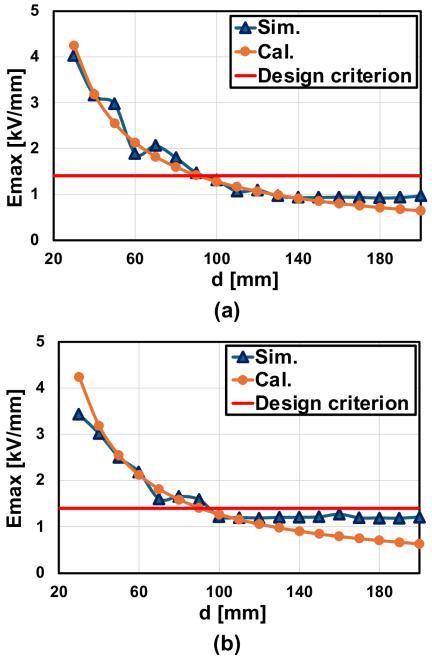
Fig. 5. Simulated maximum electric field on coil surface versus coil separation distance, \(d\), for different coil types. (a) 44-turn \(\alpha\)-wound coil. (b) 44-turn spiral coil. The applied voltage on Rx coil is 28.3 kV 9.
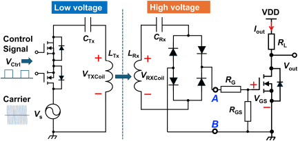
Fig. 6. Schematic of gate drive circuit using RIWPT for simulation 8.
An eddy-current solver in Ansys Maxwell is used to obtain the characteristics of the Tx and Rx coils. The coupling coefficient, \(k\), as a function of transfer distance \(d\) is simulated for 44-turn \(\alpha\)-wound and spiral coils as shown in Fig. 3. The variance of the self-inductance and parasitic resistance with respect to the carrier frequency \(f_{\mathrm{s}}\) are also simulated and demonstrated in Fig. 4. According to the simulation results, the 44-turn spiral coil exhibits a higher coupling coefficient and self-inductance than the 44-turn \(\alpha\)-wound coil, while it shows higher parasitic resistance at frequencies below 45 kHz, as shown in Fig. 4. According to 9, a galvanic insulation distance greater than 100 mm between the Tx and Rx coils is required to satisfy the design criterion for a system voltage of 28.3-kV, as illustrated in Fig. 5.
3. Circuit Schematic and Simulation Setup
The circuit schematic used for the system simulation is shown in Fig. 6. The control signal has a frequency of 100 Hz, and an amplitude of 15 V, while the carrier frequency is varied for investigation. \(L_{\mathrm{Tx}}\) and \(L_{\mathrm{Rx}}\) are the inductor on the transmitter and receiver side, respectively. Series capacitors, \(C_{\mathrm{Tx}}\) and \(C_{\mathrm{Rx}}\), are used to resonate the inductance at different carrier frequencies. \(R_{\mathrm{G}}\), \(R_{\mathrm{GS}}\) and \(R_{\mathrm{L}}\) are set to 22 \(\Omega\), 5.6 k\(\Omega\), and 100 \(\Omega\), respectively. A TW015N120C SiC power MOSFET from Toshiba (100-A rated current and 1200-V rated \(V_{\mathrm{DS}}\)) is employed as the switching device, which offers high switching speed and low switching losses 11. The main DC bus voltage is set to 1 kV. The resonant capacitors are TDK’s B3265*B series film capacitors, commonly used in snubber, resonant, and power factor correction applications, offering rated RMS voltages up to 500 V and DC ratings up to 2 kV, and maximum capacitances of approximately 150 nF 12. To provide a greater voltage margin, a capacitor bank is utilized to realize the resonant capacitance as shown in Fig. 7. High-efficiency silicon epitaxial type diodes from Toshiba are used in the full-wave rectifier 13. The rising and falling edges of the input control signal are set to \(10^{-5}\) s. Transient power electronics (PE) simulations are performed using Keysight ADS.
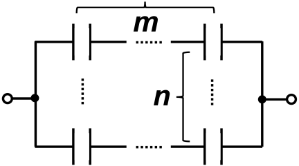
Fig. 7. Capacitor bank are used as the resonant capacitance to achieve a large voltage margin.
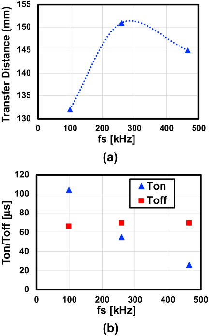
Fig. 8. Simulated results with respect to carrier frequency for the 44-turn \(\alpha\)-wound coil. (a) Transfer distance. (b) \(T_{\mathrm{on}}\) and \(T_{\mathrm{off}}\).
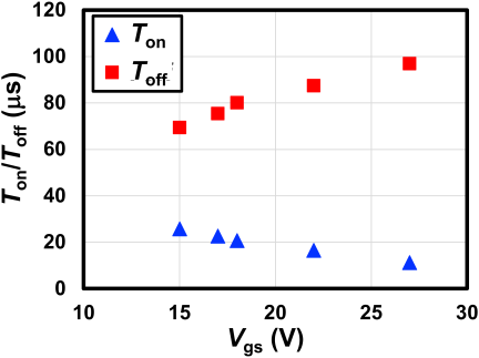
Fig. 9. Simulated \(T_{\mathrm{on}}\) and \(T_{\mathrm{off}}\) with respect to \(V_{\mathrm{GS}}\) shown in Fig. 6.
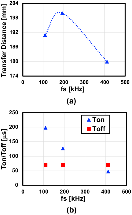
Fig. 10. Simulated results with respect to carrier frequency for the 44-turn spiral coil. (a) Transfer distance. (b) \(T_{\mathrm{on}}\) and \(T_{\mathrm{off}}\).
4. Simulation Results and Discussion
4.1. Simulation Results
The simulated results for the 44-turn \(\alpha\)-wound coil are demonstrated in Fig. 8. With a fixed control signal amplitude of 15 V and a carrier signal amplitude of 30 V, the achievable transfer distances is evaluated as a function of carrier frequency, as shown in Fig. 8(a). At these distances, a gate-source voltage \(V_{\mathrm{GS}}\) of 15 V is achieved, which is sufficient to turn-on the power transistor. A maximum transfer distance is observed near 260 kHz, indicating the existence of an optimum carrier frequency for transfer distance. The switching characteristics are also evaluated, as shown in Fig. 8(b). The turn-off time increases slightly as the carrier frequency increasing, whereas the turn-on time decreases approximately linearly. Fig. 9 further shows that \(T_{\mathrm{on}}\) and \(T_{\mathrm{off}}\) exhibit opposite dependencies on \(V_{\mathrm{GS}}\): a higher \(V_{\mathrm{GS}}\) reduce \(T_{\mathrm{on}}\) but increases \(T_{\mathrm{off}}\).
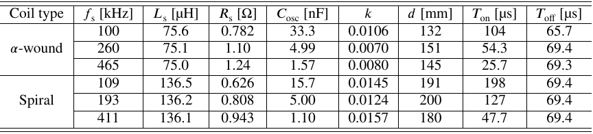
To validate these trends, the same analysis is performed for the 44-turn spiral coil. Owing to its higher coupling coefficient, the carrier signal amplitude is reduced to 10 V, compared with 30-V for the \(\alpha\)-wound coil. The simulation results are shown in Fig. 10. Despite the reduce carrier amplitude, the achievable transfer distances across the simulated carrier frequencies still satisfy the design criterion for safety galvanic insulation. In terms of switching behavior, \(T_{\mathrm{off}}\) shows negligible variation. The simulation results and corresponding parameters are summarized in Table 2.
4.2. Discussion
4.2.1. Dependence of Transfer Distance on Carrier Frequency
Although the system is maintained at resonance for all operating frequencies by adjusting the compensation capacitance, the transfer distance still exhibits a peak behavior as shown in Figs. 8(a) and 10(a). This is because the reflected impedance is proportional to \({\omega}^2M^2\), which enhances power transfer as frequency increases. However, at higher frequencies, increased AC resistance, switching losses and capacitor ESR degrade the system efficiency. The peak transfer distance therefore occurs at the frequency where the benefit of increased reflected impedance is balanced by the degradation due to frequency-dependent losses.
4.2.2. Dependence of \(T_{\mathrm{on}}\) and \(T_{\mathrm{off}}\) on Carrier Frequency
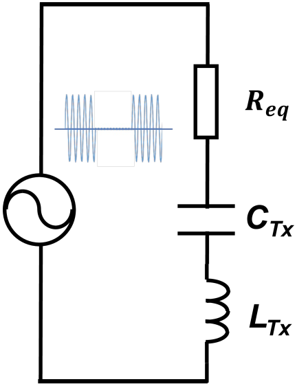
Fig. 11. The equivalent circuit of Tx.
To analyze the variation of turn-on and turn-off time with respect to carrier frequency, the low voltage side is redrawn as shown in Fig. 11. The MOSFET inverter and the carrier source \(V_\mathrm{s}\) combine to act as a high-frequency AC voltage source. \(R_{\mathrm{eq}}\) denotes the equivalent resistance when MOSFET inverter is on. Since the coupling coefficient is small, the influence of the Rx side is neglected.
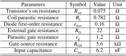
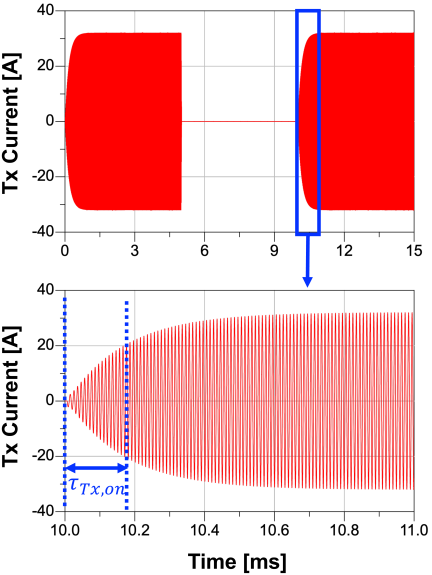
Fig. 12. Simulated Tx coil current waveform for the 44-turn \(\alpha\)-wound coil with the carrier frequency of 100 kHz.
For the 44-turns \(\alpha\)-wound coil at a carrier frequency is 100 kHz, using the parameters listed in Table 3, the calculated \(\tau_{\mathrm{Tx,on}}\) from Eq. (2) is approximately162 μs. The simulated Tx current is shown in Fig. 12, from which the simulated time constant \(\tau_{\mathrm{Tx,on}}\) is about 170 μs.
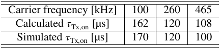
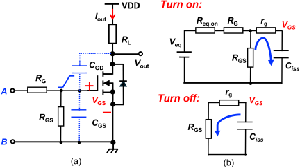
Fig. 13. The equivalent circuit of power stage.
As the carrier frequency increases, the equivalent resistance increases due to the skin effect, while the inductance remains approximately constant with this frequency range, as shown in Fig. 4(a). Consequently, the time constant decreases with frequency increasing. The simulated and calculated values of \(\tau_{\mathrm{Tx,on}}\) at different carrier frequencies are summarized in Table 4 and show good coincidence. This delay propagate to the Rx side resulting in large \(T_{\mathrm{on}}\) on the high voltage side.
In contrast, for \(\tau_{\mathrm{Tx,off}}\), the transistor exhibits an off-state resistance of several hundred M\(\Omega\), resulting in a calculated value of \(2L_{\mathrm{s}}/R_{\mathrm{eq}}\) of less than 1 ns. Consequently, the time constant \(\tau_{\mathrm{Tx,off}}\) is mainly determined by the falling edge of the control signal and the discharge process of the parasitic capacitance of the transistors. The simulated \(\tau_{\mathrm{Tx,off}}\) is approximately 12 μs for the 44-turns \(\alpha\)-wound coil at a carrier frequency of 100 kHz.
For the Rx side, when the low-voltage-side switches are on, the equivalent circuit is shown in Fig. 13, where \(V_{\mathrm{eq}}\) is the Thevenin equivalent voltage driven by the Tx side. The equivalent resistance \(R_{\mathrm{eq,on}}\) can be expressed as
When the switches are off on the low-voltage side, the transmitter tank has no excitation and there is no magnetic flux in the Tx coil, which means that no induced voltage exists on the Rx coil. Since the Rx resonant circuit has no source driving it, therefore, the diode bridge is not forward biased and no current flows through the rectifier. Looking from the load side, the rectifier diodes are reverse biased and the Rx resonant tank is floating with zero excitation, therefore, the equivalent circuit is shown as Fig. 13(b) lower part.
The time constance \(\tau_{\mathrm{Rx,on}}\) and \(\tau_{\mathrm{Rx,off}}\) based on the equivalent circuit can be expressed as:
Using the parameter listed in Table 3, \(\tau_{\mathrm{Rx,on}}\) is approximately 136 ns at the carrier frequency of 100 kHz, whereas \(\tau_{\mathrm{Rx,off}}\) is approximately 35 μs and is independent of the carrier frequency.
The overall transient behavior can be approximated by the sum of the time constants associated with the Tx and Rx sides. Since the Tx-side time constant \(\tau_{\mathrm{Tx,on}}={2L_{\mathrm{s}}}/{R_{\mathrm{eq}}}\) dominates the turn-on transient, the turn-on time is mainly determined by the Tx resonant tank. As the carrier frequency increases, the equivalent resistance \(R_{\mathrm{eq}}\) increases due to the skin effect while the inductance remains nearly constant. Consequently, \(\tau_{\mathrm{Tx,on}}\) decreases with increasing frequency. In contrast, the turn-off transient is dominated by (\(\tau_{\mathrm{Rx,off}}\)), which is determined by the Rx-side circuit and is largely independent of the carrier frequency. Therefore, the turn-on time varies with the carrier frequency, whereas the turn-off time remains nearly constant. This explains well the trends of the turn-on and turn-off times shown in Figs. 8(b) and 10(b).
4.2.3. Dependence of \(T_{\mathrm{on}}\) and \(T_{\mathrm{off}}\) on Gate Voltage
During turn-on, the MOSFET channel forms when the gate-source voltage exceeds the threshold voltage. As it is well known that the gate driver must charge the gate capacitances \(C_{\mathrm{iss}}\). The gate current is approximately
A higher gate bias voltage provides a larger gate current and faster charging of the gate capacitances. Therefore, as \(V_{\mathrm{GS}}\) increases \(T_{\mathrm{on}}\) decreases.
Since the higher gate bias voltage is achieved by increasing the coupling coefficient, the equivalent resistance reflected from the Rx side to the Tx side can be expressed as
As the coupling coefficient increases, the mutual inductance \(M\) increases, resulting in a larger reflected resistance \(R_{\mathrm{eq,Rx}}\). Consequently, the effective resistance seen by the Tx resonant circuit increases, which reduces the time constant of the Tx side. As a result, the turn-on time decreases with increasing \(V_{\mathrm{GS}}\).
During turn-off, a higher positive gate voltage results in a larger initial gate charge. Consequently, more charge must be removed before the gate voltage reaches the Miller plateau. This increases the discharge time slightly, leading to a longer turn-off time.
In summary, although an optimal carrier frequency exists for maximizing the transfer distance at a fixed gate–source voltage, the corresponding turn-on time remains relatively large. To further reduce the turn-on time, a higher carrier frequency is required. This reveals a tradeoff between transfer distance and turn-on time. For the turn-off process, a smaller \(R_{\mathrm{GS}}\) is preferred to reduce the turn-off time; however, this results in increased gate leakage current.
4.2.4. Optimization for Turn-On and Turn-Off Time
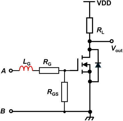
Fig. 14. Resonant gate-drive circuit with an added gate inductor 17.
Based on the above analysis, optimization of the turn-on and turn-off performance is implemented. First, a higher carrier frequency of 780 kHz and a gate drive voltage of 18 V are selected to achieve a shorter turn-on time. In addition, a gate inductor of 200 nH is introduced to resonate with the gate parasitic capacitance as shown in Fig. 14, thereby increasing the gate current and reducing \(T_{\mathrm{on}}\) 17,18,19. Furthermore, \(R_{\mathrm{G}}\) and \(R_{\mathrm{GS}}\) are reduced to 2 \(\Omega\) and 1 k\(\Omega\), respectively. The parameters used for optimization are summarized in Table 5.
With these optimizations, the turn-on and turn-off times are approximately 14 μs and 7 μs, respectively, with a transfer distance of 115 mm. To further reduce \(T_{\mathrm{on}}\) and \(T_{\mathrm{off}}\), the use of a negative gate bias voltage has been discussed in 20, although this increases system complexity.
| Parameters | Symbol | Value | Unit |
| Carrier frequency | \(f_{\mathrm{s}}\) | 780 | kHz |
| Coil parasitic resistance | \(R_{\mathrm{s}}\) | 1.3 | \(\Omega\) |
| Tx current ctrl. resistance | \(R_{\mathrm{s,Tx}}\) | 5 | \(\Omega\) |
| External gate resistance | \(R_{\mathrm{G}}\) | 2 | \(\Omega\) |
| External gate inductance | \(L_{\mathrm{G}}\) | 200 | nH |
| Gate-source resistance | \(R_{\mathrm{GS}}\) | 1 | \(\mathrm{k}\Omega\) |
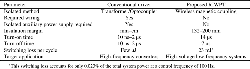
The simulated switching energy loss per cycle is approximately \(E_{\mathrm{sw}}=23\) mJ, corresponding to an average switching power loss of
The switching power loss is 2.3 W when the control signal frequency is 100 Hz. Given that the power delivered to load is approximately 10 kW, this switching loss accounts for only 0.023% of the total system power.
Although the measured turn-on and turn-off times are in the microsecond range, which are slower than those of conventional gate drivers, the proposed system is intended for high-voltage, low-switching-frequency applications where switching speed is not the primary design constraint. In applications such as pulsed power systems, high-voltage testing platforms, and solid-state protection circuits, the switching frequency is typically limited to tens or hundreds of hertz. Under these conditions, the increased switching energy has a negligible impact on the overall system efficiency. Instead, the key design requirements are reliable galvanic isolation, sufficient insulation distance, and system robustness, which are effectively addressed by the proposed RIWPT-based gate-drive approach. Therefore, the trade-off between switching speed and WPT capability is acceptable for the targeted application domain.
A comparison between conventional isolated gate drivers and the proposed RIWPT system is summarized in Table 6. Compared with conventional isolated gate drivers employing pulse transformers or optocouplers, the proposed RIWPT-based gate driver exhibits slower switching performance but offers significantly larger galvanic insulation distance. While conventional gate drivers typically achieve turn-on and turn-off times in the nanosecond-to-microsecond range, their insulation capability is limited by the transformer, optocoupler, and packaging structure. In contrast, the proposed system achieves a transfer distance of up to 200 mm while maintaining reliable gate-drive operation. Therefore, the proposed approach is particularly suitable for high-voltage and low-switching-frequency applications where insulation distance is a more critical design requirement than switching speed.
It should be noted that the results presented in this paper are based on electromagnetic simulations using Ansys Maxwell and circuit simulations using Keysight ADS. Although the fundamental operating principle of the proposed RIWPT gate-drive system has been experimentally demonstrated in our previous work, the optimized frequency characteristics investigated in this study have not yet been experimentally validated under high-voltage operating conditions. Therefore, the reported transfer distance and switching-performance results should be regarded as simulation-based design guidelines. Future work will focus on hardware implementation and experimental verification of the optimized system, including transfer-distance measurements, insulation testing, and switching-performance evaluation using high-voltage power semiconductor devices.
5. Conclusion
This paper has investigated the frequency characteristics of a high-voltage gate-drive circuit using RIWPT based on electromagnetic simulations using Ansys Maxwell and circuit simulations using Keysight ADS. For fixed control and carrier signal amplitudes, the achievable transfer distance was evaluated as a function of carrier frequency. The 44-turn \(\alpha\)-wound coil achieved a maximum transfer distance of 151 mm at a carrier frequency of 260 kHz with a 30-V carrier signal, while the spiral coil achieved 200 mm at 193 kHz with a 10-V carrier signal. Both configurations satisfy the required coil separation distance for reliable insulation at a system voltage of 28.3 kV. Furthermore, the frequency-dependent switching characteristics of the gate–source drive voltage were analyzed. It is shown that the turn-on and turn-off behaviors are governed by different mechanisms: the turn-on transient is dominated by the Tx-side time constant, which is influenced by the parasitic resistance of Tx and the reflected resistance of Rx and therefore varies with carrier frequency, whereas the turn-off transient is primarily determined by the Rx-side circuit and is largely independent of frequency. These results reveal a trade-off between transfer distance and switching performance, indicating the existence of an optimal operating frequency for high-voltage RIWPT gate-drive systems. The findings provide useful design guidelines for achieving reliable isolation and efficient switching in high-voltage applications. Since the results presented in this paper are based on simulation, experimental validation will be an important direction for future work. A prototype of the proposed RIWPT gate-drive system will be developed to verify the simulated frequency characteristics and evaluate its practical performance under high-voltage operating conditions.
Acknowledgments
This work was supported by JSPS KAKENHI Grant Number JP26K17373.
- [1] J. Rodriguez, “Multilevel inverters: a survey of topologies, controls, and applications,” IEEE Trans. on Industrial Electronics, Vol.49, No.4, pp. 724-738, 2002. https://doi.org/10.1109/TIE.2002.801052
- [2] L. Ben-Brahim, “Review of Medium Voltage High Power Electric Drives,” IEEJ J. of Industry Applications, Vol.18, No.1, pp. 1-11, 2019. https://doi.org/10.1541/ieejjia.8.1
- [3] L. Zhang, “Design Considerations for High-Voltage Insulated Gate Drive Power Supply for 10-kV SiC MOSFET Applied in Medium-Voltage Converter,” IEEE Trans. on Industrial Electronics, Vol.68, No.7, pp. 5712-5724, 2021. https://doi.org/10.1109/TIE.2020.3000131
- [4] M. V. Beigi, “Reliability, Availability, and Serviceability Challenges for Heterogeneous System Design,” 2022 IEEE Int. Reliability Physics Symposium (IRPS), pp. 2C.4-1-2C.4-8, 2022. https://doi.org/10.1109/IRPS48227.2022.9764554
- [5] T. Yoshino, “High-reliability extra-large motor drives for oil and gas industry,” 7th IEEE GCC Conf. and Exhibition (GCC), pp. 159-164, 2013. https://doi.org/10.1109/IEEEGCC.2013.6705768
- [6] R. W. Erickson and D. Maksimovic, “Fundamentals of Power Electronics,” Springer, 2020.
- [7] V. T. Nguyen, “Design of Isolated Gate Driver Power Supply in Medium Voltage Converters using High Frequency and Compact Wireless Power Transfer,” IEEE Energy Conversion Congress and Exposition (ECCE), pp. 135-142, 2019. https://doi.org/10.1109/ECCE.2019.8912184
- [8] N. Li, H. Yamamoto, Y. Okada, and T. Shinkai, “A Prototype Gate-Drive Circuit for High-Voltage Inverter Adapting Simultaneously Inductive Wireless Transfer for Both Control Signal and Power,” IEEE Access, Vol.13, pp. 16539-16547, 2025. https://doi.org/10.1109/ACCESS.2025.3530455
- [9] N. Li, Y. Okada, B. Zhang, H. Yamamoto, and T. Shinkai, “Simultaneous Galvanic Insulation and Gate Voltage Transfer for High-Voltage Power Semiconductor Operation Using Resonant Inductive Wireless Power Transfer,” IEICE Electronics Express, Vol.22, No.21, Article No.20250448, 2025. https://doi.org/10.1587/elex.22.20250448
- [10] J. He and R. S. Gorur, “Charge simulation based electric field analysis of composite insulators for HVDC lines,” IEEE Trans. on Dielectrics and Electrical Insulation, Vol.21, pp. 2541-2548, 2014. https://doi.org/10.1109/TDEI.2014.004541
- [11] MOSFETs Silicon Carbide N-Channel MOS TW015N120C (2024). https://toshiba.semicon-storage.com/info/docget.jsp?did=143221 [Accessed July 1, 2025]
- [12] https://www.tdk-electronics.tdk.com/en/3191426/products/product-catalog/film-capacitors/capacitors-for-snubbering-resonant-circuits-pfc [Accessed July 1, 2025]
- [13] https://www.tyro-teq.com/ic/product/TOSHIBA/CMH01 [Accessed July 1, 2025]
- [14] M. F. Mahmood, S. L. Mohammed, S. K. Gharghan, A. Al-Naji, and J. Chahl, “Hybrid Coils-Based Wireless Power Transfer for Intelligent Sensors,” Sensors, Vol.20, No.9, Article No.2549, 2020. https://doi.org/10.3390/s20092549
- [15] H. Feng, T. Cai, S. Duan, J. Zhao, X. Zhang, and C. Chen, “An LCC-Compensated Resonant Converter Optimized for Robust Reaction to Large Coupling Variation in Dynamic Wireless Power Transfer,” IEEE Trans. on Industrial Electronics, Vol.63, No.10, pp. 6591-6601, 2016. https://doi.org/10.1109/TIE.2016.2589922
- [16] N. Li, K. Iguchi, X. Liu, A. Shirane, K. Okada, and T. Shinkai, “Conductive and Capacitive Properties of Couplers under Seawater for Electric Wireless Power Transfer,” 2024 IEEE Wireless Power Technology Conf. and Expo (WPTCE), pp. 308-311, 2024. https://doi.org/10.1109/WPTCE59894.2024.10557356
- [17] H. Fujita, “A resonant gate-drive circuit capable of high-frequency and high-efficiency operation,” 2009 IEEE 6th Int. Power Electronics and Motion Control Conf., pp. 351-357, 2009. https://doi.org/10.1109/IPEMC.2009.5157411
- [18] H. Fujita and M. Ishigaki, “A resonant gate-drive circuit with optically-isolated control signal and power supply for fast-switching and high-voltage power semiconductor devices,” The 2010 Int. Power Electronics Conf. (ECCE ASIA), pp. 1895-1901, 2010. https://doi.org/10.1109/IPEC.2010.5542024
- [19] W. Eberle, Y.-F. Liu, and P. C. Sen, “A New Resonant Gate-Drive Circuit With Efficient Energy Recovery and Low Conduction Loss,” IEEE Trans. on Industrial Electronics, Vol.55, No.5, pp. 2213-2221, 2008. https://doi.org/10.1109/TIE.2008.918636
- [20] Y. Okada, N. Li, and T. Shinkai, “Bipolarization of Gate Signal of High-Voltage Power Semiconductors Transmitted by Wireless Power Transfer,” IEEE Access, Vol.13, pp. 200995-201005, 2025. https://doi.org/10.1109/ACCESS.2025.3637017
This article is published under a Creative Commons Attribution-NoDerivatives 4.0 Internationa License.